Sensor LGA (Land Grid Array) packaging structure

A technology of LGA packaging and packaging structure, which is applied in the direction of semiconductor devices, electrical solid devices, semiconductor/solid device components, etc., can solve problems affecting product performance, large internal stress, high cost, etc., and reduce electrical signal data drift and barrier effect of influence

Inactive Publication Date: 2018-11-13
无锡韦感半导体有限公司
View PDF7 Cites 2 Cited by
  • Summary
  • Abstract
  • Description
  • Claims
  • Application Information

AI Technical Summary

Problems solved by technology

In order to improve the characteristics of sensor products, for example, the patent CN201383873Y makes the silicon capacitor microphone have higher sensitivity and better frequency response curve in its acoustic-electric conversion by setting gaskets. At present, there are many kinds of gasket materials commonly used in the industry, including Glass, ceramics, copper (nickel-plated or gold-plated), PCB substrate, and stainless steel, etc. In addition, if copper (nickel-plated or gold-plated) or PCB substrate is used for connection, welding is often the preferred method, such as patent CN205122573U, although welding production The efficiency is high, but if the pads are made on the PCB substrate or metals such as solderable gold / nickel are plated on the copper, the cost is relatively high, and the temperature of the tin metal during the soldering process is as high as 250-300°C, which will experience liquefaction And the curing process will cause a large change in the shape / shrinkage of the tin, which may generate a large internal stress, thereby affecting the final performance of the product

Method used


Image

  • Sensor LGA (Land Grid Array) packaging structure

Examples


Embodiment Construction

[0022] The implementation of the present invention will be described in detail below with examples and accompanying drawings, so as to fully understand and implement the process of how to apply technical means to solve technical problems and achieve technical effects in the present invention.

[0023] The embodiment of the present invention discloses a sensor LGA packaging structure, so as to optimize the electrical signal drift problem of the transducer chip output caused by the influence of substrate stress during mass production.

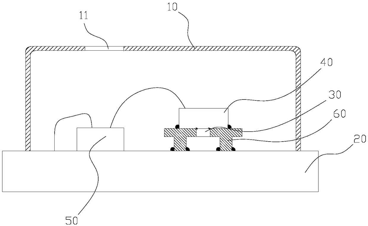
[0024] Such as figure 1 As shown, the sensor LGA packaging structure of this embodiment includes a housing 10 and a substrate 20, the substrate 20 and the housing 10 form a packaging structure, the packaging structure is used to package the transducer chip 40, and the sensor LGA packaging structure also includes a gasket 60, The gasket 60 is used to bond the transducer chip 40, and the bonding adopts an adhesive method. The upper and lower surfac...


PUM


Abstract

The invention provides a sensor LGA (Land Grid Array) packaging structure which comprises a shell and a substrate. The packaging structure is used for packaging an energy converter chip; the sensor LGA packaging structure also comprises a gasket; the gasket is used for adhering to the energy converter chip; a through hole is formed in the gasket in a way of penetrating through the upper surface and the lower surface; for the lower surface, connected with the substrate, of the bottom part of the gasket, due to the through hole, other areas of the gasket is adhered to the substrate through a glue. During the mass production of the packaging structure, the stress of the substrate can be optimized through the method, and the drifting problem of an electric signal output by the energy converterchip caused by the stress is solved.

Description

technical field [0001] The present invention relates to the field of sensor packaging, more specifically, to a sensor LGA packaging structure. Background technique [0002] Packaging technology is crucial for chips. At present, the packaging technology of semiconductor chips covers Filp Chip, COB and LGA in various forms. Among them, in view of the good performance of LGA packaging technology in terms of its interface richness, mechanical stability and heat dissipation, it has received more and more attention and attention. application. The full name of LGA is Land Grid Array, or flat grid array package, which belongs to the surface mount technology of integrated circuits (IC). Chips in this package are often connected or directly soldered to a printed circuit board (PCB substrate) superior. [0003] Specific to the LGA structure packaging of sensors, such as silicon microphones, pressure gauges, infrared sensors, thermometers, etc., the metal shell is often welded to the...

Claims


Application Information

Patent Timeline
IPC IPC(8): H01L23/057H01L23/13H01L25/18
CPCH01L25/18H01L23/057H01L23/13H01L2224/73265H01L2224/48137H01L2924/16152H01L2924/16151
Inventor 万蔡辛
Owner 无锡韦感半导体有限公司
Why Eureka
Try Eureka