Light-emitting diode epitaxial wafer and preparation method thereof

A technology for light-emitting diodes and epitaxial wafers, applied in electrical components, circuits, semiconductor devices, etc., can solve the problems of low luminous efficiency of light-emitting diodes, and achieve the effects of increasing recombination efficiency, increasing luminous efficiency, and increasing the number of holes

Active Publication Date: 2018-11-13
HC SEMITEK ZHEJIANG CO LTD
View PDF5 Cites 7 Cited by
  • Summary
  • Abstract
  • Description
  • Claims
  • Application Information

AI Technical Summary

Problems solved by technology

But at the same time, the AlGaN electron blocking layer will also prevent holes from entering the active layer. The number of holes entering the active layer is originally less than the number of electrons entering the active layer. The AlGaN electron blocking layer will limit the entry into the active layer. The number of holes makes the number of holes that coincide with electrons in the active layer to emit light less, making the overall luminous efficiency of the light-emitting diode lower

Method used


Image

  • Light-emitting diode epitaxial wafer and preparation method thereof
  • Light-emitting diode epitaxial wafer and preparation method thereof
  • Light-emitting diode epitaxial wafer and preparation method thereof

Examples


Embodiment Construction

[0031] In order to make the object, technical solution and advantages of the present invention clearer, the implementation manner of the present invention will be further described in detail below in conjunction with the accompanying drawings.

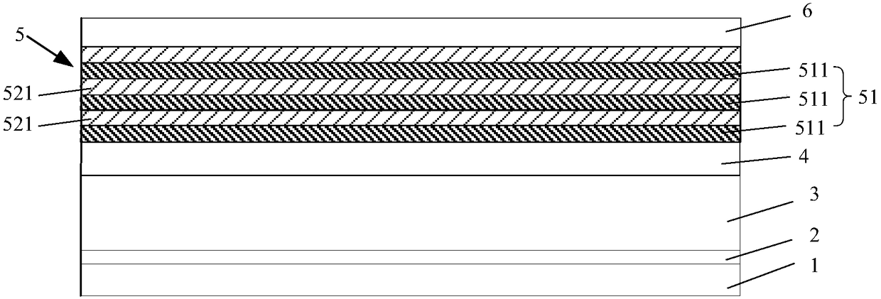
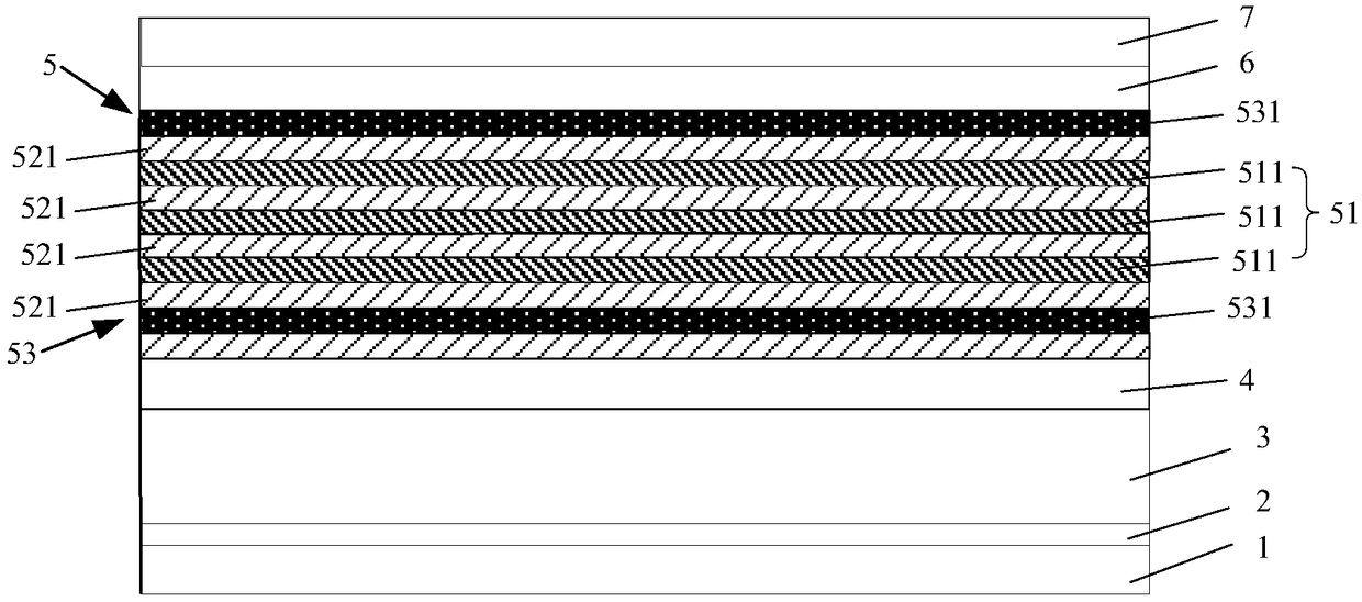
[0032] figure 1 It is a structural diagram of a light-emitting diode epitaxial wafer provided by an embodiment of the present invention. Such as figure 1 As shown, the epitaxial wafer includes a substrate 1 and a low-temperature GaN buffer layer 2 , an undoped GaN layer 3 , an N-type GaN layer 4 , an active layer 5 and a P-type GaN layer 6 sequentially stacked on the substrate 1 .

[0033] The active layer 5 includes a first barrier layer 51 and a plurality of well layers 521, the first barrier layer 51 includes a plurality of first sub-barrier layers 511, the first sub-barrier layers 511 and the well layers 521 are alternately stacked, and the well layers 521 are InGaN well layer, the first sub-barrier layer 511 includes GaN / In x G...


PUM


Abstract

The invention discloses a light-emitting diode epitaxial wafer and a preparation method thereof and belongs to the field of light-emitting diode manufacturing. An active layer is arranged to include afirst barrier layer and a plurality of InGaN well layers, wherein a plurality of first sub-barrier layers with a GaN / In<x>Ga<1-x>N / Al<z>Ga<1-z>N / In<y>Ga<1-y>N / GaN superlattice structure in the firstbarrier layer and the InGaN well layers are alternately stacked. The GaN / In<x>Ga<1-x>N / Al<z>Ga<1-z>N / In<y>Ga<1-y>N / GaN superlattice structure is relatively high in energy band and can play a role in preventing electrons from entering a P-type GaN layer, so that an electron blocking layer does not need to be arranged to prevent the electrons from flowing out of an active layer. Through the arrangement, the number of holes entering the active layer can be improved while the electrons are restricted from leaving the active layer, so that the number of the holes which are compounded with the electrons to emit light in the active layer is improved; and furthermore, the polarization condition, caused by the arrangement of the electron blocking layer, between the electron blocking layer and the active layer and the P-type layer in an epitaxial layer can also be reduced, so that reduction of a light-emitting band gap in the epitaxial layer is avoided and the recombination efficiency of the electrons and the holes is improved, thereby improving the light-emitting efficiency of a light-emitting diode.

Description

technical field [0001] The invention relates to the field of light-emitting diode manufacturing, in particular to a light-emitting diode epitaxial wafer and a preparation method thereof. Background technique [0002] Light-emitting diodes are semiconductor diodes that can convert electrical energy into light energy. They have the advantages of small size, long life, and low power consumption. They are currently widely used in automotive signal lights, traffic lights, display screens, and lighting equipment. The epitaxial wafer is the basic structure for making light-emitting diodes. The structure of the epitaxial wafer includes a substrate and an epitaxial layer grown on the substrate. Among them, the structure of the epitaxial layer mainly includes: a low-temperature GaN buffer layer, an undoped GaN layer, an N-type GaN layer, an active layer, an AlGaN electron blocking layer and a P-type GaN layer grown on the substrate in sequence. [0003] The AlGaN electron blocking la...

Claims


Application Information

Patent Timeline
Patent Type & Authority Applications(China)
IPC IPC(8): H01L33/06H01L33/12H01L33/32H01L33/00
CPCH01L33/0075H01L33/06H01L33/12H01L33/32
Inventor 刘旺平乔楠
Owner HC SEMITEK ZHEJIANG CO LTD
Why Eureka
Try Eureka