Supercharge Your Innovation With Domain-Expert AI Agents!

DC boost circuit and DC boost method

一种直流升压电路、电阻的技术,应用在直流功率输入变换为直流功率输出、电气元件、调节电变量等方向,能够解决影响有机发光二极管电流大小、影响OLED显示器显示质量等问题,达到电压准位稳定、补偿压降、保证电压准位的效果

Active Publication Date: 2019-07-02
SHENZHEN CHINA STAR OPTOELECTRONICS SEMICON DISPLAY TECH CO LTD
View PDF5 Cites 0 Cited by
  • Summary
  • Abstract
  • Description
  • Claims
  • Application Information

AI Technical Summary

Problems solved by technology

When the OLED display displays different pictures, the load current of the DC boost circuit is different, so the positive voltage of the power supply received by the pixel drive circuit is different, which will affect the current of the organic light-emitting diode flowing through each pixel, and then affect the display quality of the OLED display.

Method used


Image

  • DC boost circuit and DC boost method
  • DC boost circuit and DC boost method
  • DC boost circuit and DC boost method

Examples


Embodiment Construction

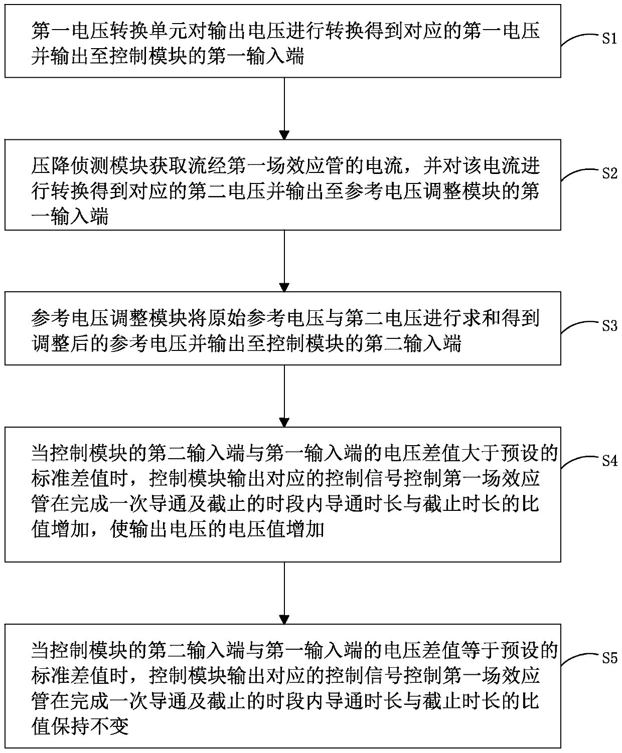
[0044] In order to further illustrate the technical means adopted by the present invention and its effects, the following describes in detail in conjunction with preferred embodiments of the present invention and accompanying drawings.

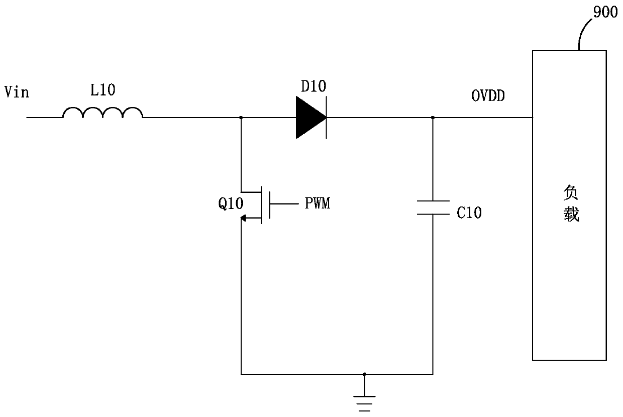
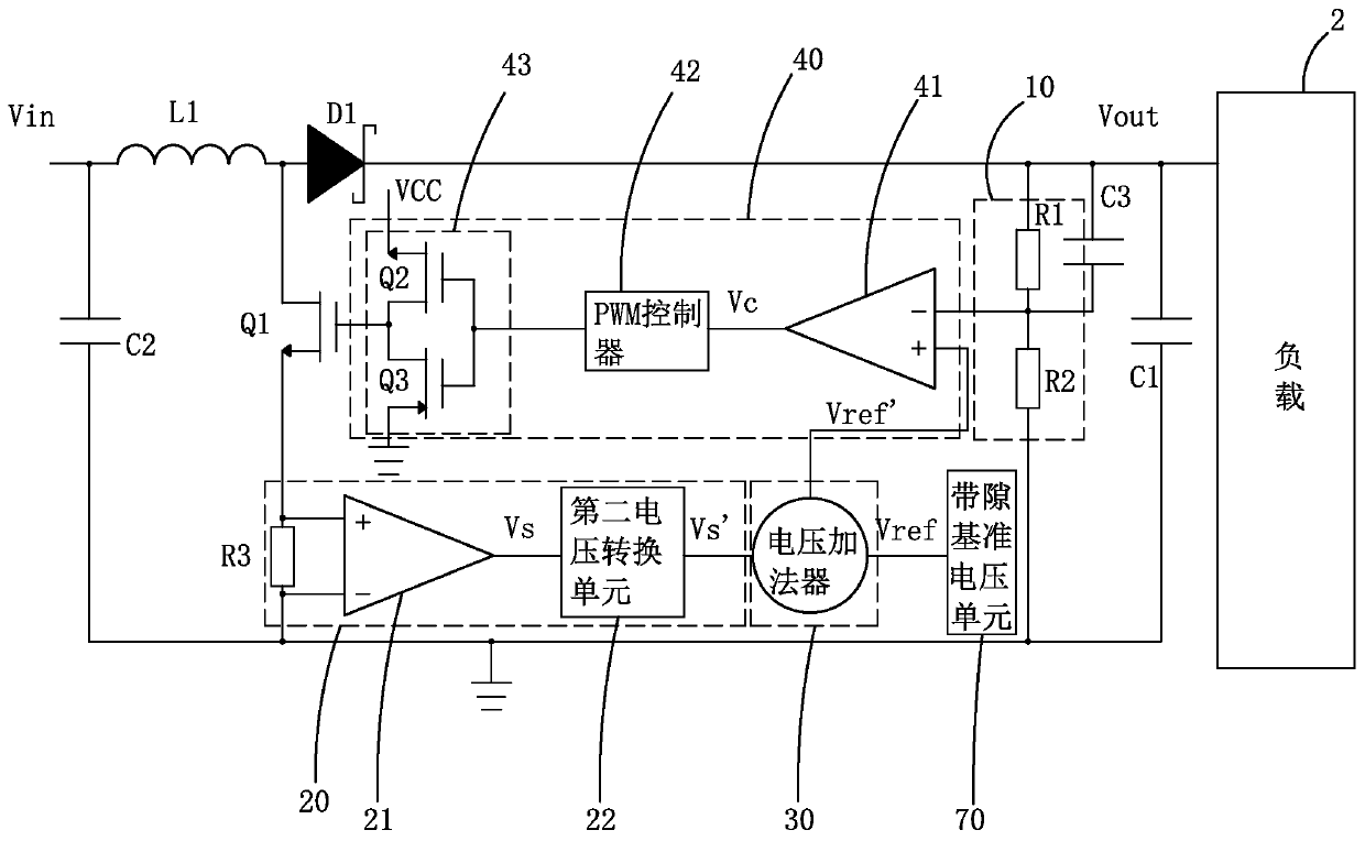
[0045] see figure 2 A DC boost circuit provided by the present invention includes an inductor L1, a diode D1, a first capacitor C1, a first field effect transistor Q1, a first voltage conversion unit 10, a voltage drop detection module 20, a reference voltage adjustment module 30 and control module 40 .

[0046] The first end of the inductor L1 is connected to the input voltage Vin, and the second end is electrically connected to the anode of the diode D1. The cathode of the diode D1 is electrically connected to the load 2 and transmits the output voltage Vout to the load 2 . The first terminal of the first capacitor C1 is electrically connected to the cathode of the diode D1, and the second terminal is grounded. The drain of the first fie...


PUM


Abstract

The invention provides a DC boosting circuit and a DC boosting method. The DC boost circuit of the present invention includes an inductor, a diode, a first capacitor, a first field effect transistor, a first voltage conversion unit, a voltage drop detection module, a reference voltage adjustment module and a control module. After the load is connected, the voltage drop detection module obtains the current flowing through the diode and outputs the corresponding second voltage to the reference voltage adjustment module, so that the voltage output by the reference voltage adjustment module is greater than the original reference voltage, and the control module controls the first field The increase of the ratio of the on-time length to the off-time length of the effect tube in the period of completing a turn-on and cut-off time increases the voltage value of the output voltage, thereby compensating the voltage drop of the output voltage caused by the impedance and ensuring the voltage level of the output voltage is stable. .

Description

technical field [0001] The invention relates to the field of display technology, in particular to a DC boost circuit and a DC boost method. Background technique [0002] Organic light emitting diode (Organic Light Emitting Display, OLED) display device has self-illumination, low driving voltage, high luminous efficiency, short response time, high definition and contrast, nearly 180° viewing angle, wide operating temperature range, and can realize flexible display and With many advantages such as large-area full-color display, it is recognized by the industry as a display device with the most potential for development. [0003] OLED display devices can be divided into passive matrix OLED (Passive Matrix OLED, PMOLED) and active matrix OLED (Active Matrix OLED, AMOLED) two categories according to the driving method, namely direct addressing and thin film transistor (Thin Film Transistor, TFT) matrix addressing two types. Among them, AMOLED has pixels arranged in an array, be...

Claims


Application Information

Patent Timeline
Patent Type & Authority Patents(China)
IPC IPC(8): H02M3/156
CPCH02M3/156G09G3/3225G09G2330/02H02M1/08H03F3/2173H03F3/45475H03F2200/351G09G3/3233G09G2320/0204H02M3/155
Inventor 常勃彪
Owner SHENZHEN CHINA STAR OPTOELECTRONICS SEMICON DISPLAY TECH CO LTD
Features
  • R&D
  • Intellectual Property
  • Life Sciences
  • Materials
  • Tech Scout
  • Unparalleled Data Quality
  • Higher Quality Content
  • 60% Fewer Hallucinations
Learn More