Array substrate and liquid crystal display panel

An array substrate and substrate technology, applied in optics, instruments, electrical components, etc., can solve the problems of large difference in birefringence of liquid crystal molecules, loss of aperture ratio, serious color shift, etc., to reduce energy consumption, increase brightness, and increase area. Effect

Inactive Publication Date: 2020-09-18
SHENZHEN CHINA STAR OPTOELECTRONICS SEMICON DISPLAY TECH CO LTD
View PDF7 Cites 7 Cited by
  • Summary
  • Abstract
  • Description
  • Claims
  • Application Information

AI Technical Summary

Problems solved by technology

However, since the VA mode uses vertically rotating liquid crystals, the difference in birefringence of liquid crystal molecules is relatively large, resulting in serious color shift problems at large viewing angles.
[0003] At present, in order to improve the viewing angle performance of the panel, the PSVA pixel design of 3T-8domain (8 domains and 3 transistors) is usually used. However, in 3T-8domain (8 domains and 3 transistors), a display panel with a VA pixel structure driven by 3 TFTs is required. , although this design can increase the viewing angle, it will lose the aperture ratio, and at the same time require the backlight to provide higher brightness, resulting in an increase in power consumption

Method used


Image

  • Array substrate and liquid crystal display panel
  • Array substrate and liquid crystal display panel
  • Array substrate and liquid crystal display panel

Examples


Embodiment Construction

[0028] The technical solutions in the embodiments of the present application will be clearly and completely described below in conjunction with the drawings in the embodiments of the present application. Apparently, the described embodiments are only some of the embodiments of this application, not all of them. Based on the embodiments in this application, all other embodiments obtained by those skilled in the art without making creative efforts belong to the scope of protection of this application.

[0029] In the description of the present application, it should be understood that the terms "center", "longitudinal", "transverse", "length", "width", "thickness", "upper", "lower", "front", " Orientation indicated by rear, left, right, vertical, horizontal, top, bottom, inside, outside, clockwise, counterclockwise, etc. The positional relationship is based on the orientation or positional relationship shown in the drawings, which is only for the convenience of describing the a...


PUM


Abstract

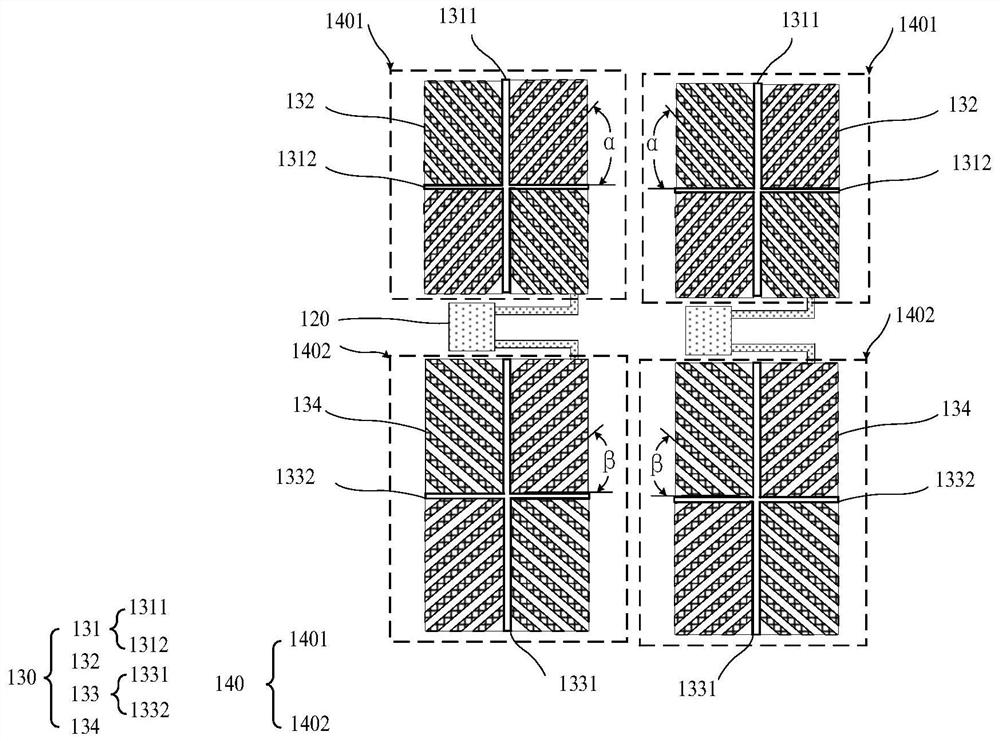
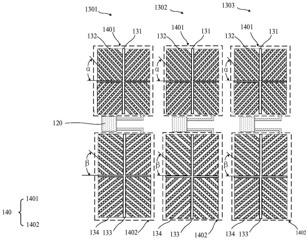
The invention provides an array substrate and a liquid crystal display panel. The array substrate comprises a substrate body, a thin film transistor layer located on the substrate body and a pixel electrode located on the thin film transistor layer. The array substrate comprises a plurality of sub-pixel areas, and each sub-pixel area comprises a main area and an auxiliary area. The pixel electrodes are arranged corresponding to the main area and the auxiliary area, and each pixel electrode comprises a first main electrode and a first branch electrode which correspond to the main area, and a second main electrode and a second branch electrode which correspond to the auxiliary area; the first branch electrode is electrically connected with the first main electrode at a first preset angle;thesecond branch electrode is electrically connected with the second main electrode at a second preset angle;and the first preset angle is different from the second preset angle. By controlling the angle of the pixel electrode, the number of thin film transistors in the prior art is reduced, the pixel aperture opening ratio and transmittance are increased, and meanwhile the wide viewing angle effectof the liquid crystal display panel is achieved.

Description

technical field [0001] The present application relates to the field of display technology, in particular to an array substrate and a liquid crystal display panel. Background technique [0002] A liquid crystal display panel is usually composed of a color filter substrate, a thin film transistor array substrate, and a liquid crystal layer disposed between the two substrates, including twisted nematic (TN) mode, electronically controlled birefringence (ECB) mode, vertical alignment (VA) Among them, the VA mode is a common display mode with the advantages of high contrast, wide viewing angle, and no need for frictional alignment. However, since the vertically rotating liquid crystal is used in the VA mode, the difference in birefringence of the liquid crystal molecules is relatively large, resulting in serious color shift problems at large viewing angles. [0003] At present, in order to improve the viewing angle performance of the panel, the PSVA pixel design of 3T-8domain (8...

Claims


Application Information

Patent Timeline
Patent Type & Authority Applications(China)
IPC IPC(8): G02F1/1343G02F1/1368H01L27/12
CPCG02F1/134309G02F1/1368H01L27/1214G02F2201/40
Inventor 张翼鹤
Owner SHENZHEN CHINA STAR OPTOELECTRONICS SEMICON DISPLAY TECH CO LTD
Why Eureka
Try Eureka