Optical module

A technology of an optical module and an arrayed waveguide grating, which is applied in the field of optical communication, can solve the problems of reducing the space where the circuit board 30 is coated with glue, the surface of the circuit board 30 being scratched, and affecting the coupling performance of the receiving end.

Inactive Publication Date: 2018-11-16
HISENSE BROADBAND MULTIMEDIA TECH
View PDF3 Cites 8 Cited by
  • Summary
  • Abstract
  • Description
  • Claims
  • Application Information

AI Technical Summary

Problems solved by technology

[0004] 1. When the light is transmitted from the mirror to the PD array receiving chip, due to the change of the transmission medium, the light is transmitted from the bottom surface of the mirror at an angle of outward diffusion. If the L size is too large, it will reduce the reception of the PD array receiving chip. The number of light rays affects the coupling performance of the receiving end;
[0005] In order to ensure the coupling performance of the receiving end, the distance between the bottom surface of the reflector 12 and the PD receiving chip 13 arranged on the circuit board 30 is reduced. If the distance between the surface of the board 30 is too small, or even interfere with it, on the one hand, it will scratch the surface of the circuit board 30, and on the other hand, it will reduce the space for coating the glue on the circuit board 30. Can not guarantee the fixed stability of arrayed waveguide grating 11

Method used


Image

  • Optical module
  • Optical module
  • Optical module

Examples


Embodiment Construction

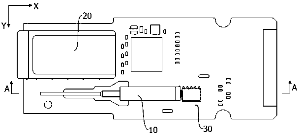
[0019] In the existing optical module structure, in order to ensure the signal isolation between the transmitting end and the receiving end, to reduce the mutual crosstalk of the signals transmitted by the transmitting end and the receiving end, the receiving end and the transmitting end are staggered on the circuit board to increase the receiving end. The distance between the terminal and the transmitting terminal, but due to the large number of components at the transmitting terminal and the driver chip arranged behind it, furthermore, limited by the width of the circuit board, it cannot be in the width direction (see Figure 1a middle Y direction) to increase the distance between the transmitter and the receiver, please refer to Figure 1a As shown, the receiving end 10 is arranged along the side towards the electric port of the circuit board 30, that is, the receiving end is arranged along the Figure 1a The middle X direction is set away from the transmitting end 20, increas...


PUM


Abstract

The invention provides an optical module. The optical module comprises a circuit board, and an array waveguide grating, a reflector, and a PD array reception chip arranged on the circuit board, the array waveguide grating is connected with the reflector, the PD array reception chip is electrically connected with the circuit board, the PD array reception chip is used for receiving light transmittedby the array waveguide grating and emitted by the reflector, the array waveguide grating and the reflector are arranged opposite to the circuit board in a height direction of the circuit board, the circuit board is provided with a sunk groove arranged along the height direction of the circuit board, the array waveguide grating is arranged opposite to the sunk groove in the height direction of thecircuit board, and the array waveguide grating is fixedly arranged in the sunk groove. The circuit board is provided with the recessed sunk groove along the height direction of the circuit board so that the coupling space of the array waveguide grating and the reflector in the height direction can be increased, the distance from the bottom surface of the reflector to the PD array reception chip is shortened, the coupling performance of a receiving end is enhanced, the sunk groove can increase the space, used for fixing the array waveguide grating, of the circuit board, and the fixing stability of the array waveguide grating is improved.

Description

technical field [0001] The invention relates to the technical field of optical communication, in particular to an optical module. Background technique [0002] Optical modules are key components in optical networks. The optical module includes a transmitting end and a receiving end. The transmitting end converts the electrical signal into an optical signal and transmits it through an optical fiber. The receiving end converts the received optical signal into an electrical signal. In order to ensure the signal isolation between the transmitting end and the receiving end, in order to reduce the mutual crosstalk of the signals transmitted by the transmitting end and the receiving end, the receiving end and the transmitting end are staggered on the circuit board to increase the distance between the receiving end and the transmitting end. Reduce signal crosstalk between the two. Due to the large number of components at the transmitting end and the driver chip behind it, and limi...

Claims


Application Information

Patent Timeline
Patent Type & Authority Applications(China)
IPC IPC(8): G02B6/42G02B6/12
CPCG02B6/12009G02B6/4214G02B6/428G02B6/4287
Inventor 谢一帆傅钦豪刘维伟付孟博
Owner HISENSE BROADBAND MULTIMEDIA TECH
Why Eureka
Try Eureka