Low-dynamic maladjusted high-speed low-power consumption comparator circuit
A comparator circuit and low power consumption technology, which is applied in the field of high-speed and low-power comparator circuits, can solve problems such as large dynamic imbalance of comparator circuits, and achieve the effects of reducing complexity, improving stability, and increasing speed
- Summary
- Abstract
- Description
- Claims
- Application Information
AI Technical Summary
Problems solved by technology
Method used
Image
Examples
Embodiment 1
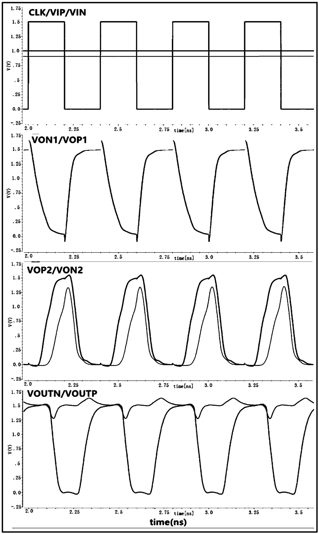
[0052] see Figure 5 , The low dynamic offset high-speed low-power comparator circuit of this embodiment includes a first-stage pre-amplification circuit and a second-stage positive feedback latch circuit. The comparator circuit of this embodiment uses the clock signal CLK to control the comparison phase and the reset phase of the comparator circuit.
[0053] When the clock signal CLK is at a high level, the comparator circuit is in the comparison stage, and a pair of differential input signals VIP and VIN are respectively amplified by the first-stage pre-amplification circuit to form a pair of one-stage differential signals VON1 and VOP1; the second-stage positive feedback latch The circuit inverts and amplifies a pair of first-level differential signals VON1 and VOP1 to form a pair of second-level differential signals VOP2 and VON2, and performs positive feedback latching on the second-level differential signals VOP2 and VON2 to obtain a pair of differential output signals V...
Embodiment 2
[0057] This embodiment specifically designs the first-stage pre-amplification circuit, wherein the first-stage pre-amplification circuit includes a tail current source circuit, a cascode switch circuit, a pair of differential input circuits, and a pair of reset circuits.
[0058] The tail current source circuit is biased by the bias voltage VB and outputs a tail current source.
[0059] The cascode switching circuit transmits the tail current source under the control of the clock signal CLK.
[0060] In the comparison stage, a pair of differential input circuits respectively amplifies the differential input signals VIP and VIN according to the tail current source to form primary differential signals VON1 and VOP1.
[0061] A pair of reset circuits set the primary differential signals VON1 and VOP1 in the reset phase.
[0062] Therefore, the high-speed low-power comparator circuit with low dynamic offset of this embodiment uses the bias voltage to bias the tail current source ...
Embodiment 3
[0064] see Image 6 , this embodiment is illustrated on the basis of Embodiment 2, wherein the tail current source circuit uses a tail current source tube Mtail, the cascode switch circuit uses a cascode switch tube Mclk, and a pair of differential input circuits uses a For the differential input transistors MN1 and MN2, a pair of reset transistors MP1 and MP2 are used for a pair of reset circuits. The tail current source tube Mtail, the cascode switch tube Mclk, the differential input tubes MN1 and MN2 are all NMOS tubes, and the reset tubes MP1 and MP2 are all PMOS tubes. The specific connection mode inside the first stage pre-amplification circuit in this embodiment is as follows:
[0065] The source of the tail current source tube Mtail is grounded, the gate is connected to the bias voltage VB, and the drain is connected to the source of the cascode switch Mclk.
[0066] The gate of the cascode switch Mclk is connected to the clock signal CLK, and the drain of the cascod...
PUM
 Abstract
Description
Claims
Application Information


