3D printing method for ceramic substrate multilayer circuit

A 3D printing, ceramic substrate technology, applied in printed circuits, circuit substrate materials, printed circuit manufacturing, etc., to achieve the effect of high production efficiency

Inactive Publication Date: 2018-11-16
DONGGUAN INST OF OPTO ELECTRONICS PEKING UNIV
View PDF3 Cites 3 Cited by
  • Summary
  • Abstract
  • Description
  • Claims
  • Application Information

AI Technical Summary

Problems solved by technology

However, the current ceramic metallization process can only be limited to making circuits on the front and back surfaces of ceramics (the two layers of circuits are connected by laser drilling, connected by electroplating, chemical plating, etc.), that is, only two layers can be made at most. circuit

Method used


Image

  • 3D printing method for ceramic substrate multilayer circuit
  • 3D printing method for ceramic substrate multilayer circuit
  • 3D printing method for ceramic substrate multilayer circuit

Examples


Embodiment 1

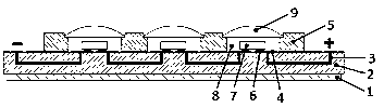
[0027] as attached figure 1 Shown, a kind of 3D printing method of ceramic substrate multilayer circuit, comprises the following steps:

[0028] S1, first draw the model with 3D drawing software according to the design requirements, and convert it into a file format that the 3D printer can recognize.

[0029] S2. On the copper substrate 1, the 3D printer sprays a certain thickness of ceramic slurry to form a ceramic substrate 2, and waits for it to solidify.

[0030] S3. Then replace the nozzle of the 3D printer, and print a layer of conductive paste on the surface of the ceramic substrate according to the circuit design requirements to form a circuit 3 with a certain thickness and a certain width.

[0031] S4, and then print a layer of flat ceramic slurry on the circuit to form a ceramic thin material layer, so that it covers the circuit.

[0032] S5. Replace the printing nozzle, and print the chip pad 4, the power supply external pad 6 and other connecting lines on the sur...

Embodiment 2

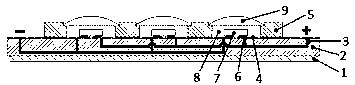
[0036] as attached figure 2 As shown, the preparation of this embodiment is basically the same as that of the first embodiment, the difference is that when printing the circuit 3, two layers of disjoint circuits are printed to meet different requirements.

Embodiment 3

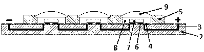
[0038] as attached image 3 As shown, compared with Embodiment 1, this embodiment lies in that the ceramic substrate is directly printed without using a copper substrate, and specifically includes the following steps:

[0039] S1, first draw the model with 3D drawing software according to the design requirements, and convert it into a file format that the 3D printer can recognize.

[0040] S2. The 3D printer sprays a certain thickness of ceramic slurry to form the ceramic substrate 2, and waits for it to solidify.

[0041] S3. Then replace the nozzle of the 3D printer, and print a layer of circuit paste on the surface of the ceramic substrate according to the circuit design requirements to form a circuit 3 with a certain thickness and a certain width.

[0042] S4, and then print a layer of flat ceramic slurry on the circuit to form a ceramic thin material layer, so that it covers the circuit.

[0043] S5. Replace the printing nozzle, and print the chip pad 4, the power suppl...


PUM


Abstract

A 3D printing method for a ceramic substrate multilayer circuit comprises the steps of: drawing a model by using three-dimensional drawing software according to a design requirement and converting themodel into a file format recognizable by a 3D printing device; printing a flat ceramic slurry layer having a predetermined thickness on a copper substrate to form a ceramic substrate in order to support a circuit to be printed in the next step; moving a printing nozzle according to a printing path, spraying a conductive paste layer onto the ceramic substrate, and irradiating the conductive pastelayer with ultraviolet light in order that the conductive paste layer is solidified into the circuit; spraying the ceramic slurry onto the circuit to print a ceramic thin layer which covers the entirecircuit; according to a preset requirement, arranging a chip bonding pad, a power supply bonding pad and connection lines on the ceramic thin layer; disposing a cup on the ceramic thin layer and thenspraying a reflective layer material around the inner wall of the cup; and removing the ceramic substrate from the 3D printing device. The method has high production efficiency and can realize processing of a multilayer circuit.

Description

technical field [0001] The invention relates to the field of manufacturing technologies of aluminum nitride and alumina ceramic substrates, in particular to a 3D printing method for multilayer circuits of ceramic substrates. Background technique [0002] The advent of ceramic substrate products has opened the development of the heat dissipation application industry. Due to the heat dissipation characteristics of ceramic substrates, and the advantages of high heat dissipation, low thermal resistance, long life, and withstand voltage, ceramic substrates are widely used in various fields such as LED packaging, power electronic devices, and multi-chip modules. With the improvement of production technology and equipment, the rationalization of product prices has accelerated, and the application fields of the LED industry have been expanded, such as indicator lights for home appliances, car lights, street lights, and large outdoor billboards. The successful development of ceramic...

Claims


Application Information

Patent Timeline
Patent Type & Authority Applications(China)
IPC IPC(8): H05K3/00H05K3/12H05K1/03
CPCH05K3/0011H05K1/0306H05K3/1275
Inventor 杨功寿郑小平李成明陈建倪绿军王琦张国义
Owner DONGGUAN INST OF OPTO ELECTRONICS PEKING UNIV
Why Eureka
Try Eureka