Hole forming method

An amorphous carbon and material layer technology, applied in the manufacture of electrical components, electrical solid devices, semiconductor/solid devices, etc., can solve the problems of storage electron density limit, development technology limit, etc., to avoid the difference between the bottom size and the top size Large variance, cost reduction, and improved effect of inconsistent aperture roundness

Inactive Publication Date: 2018-11-20
YANGTZE MEMORY TECH CO LTD
View PDF5 Cites 2 Cited by
  • Summary
  • Abstract
  • Description
  • Claims
  • Application Information

AI Technical Summary

Problems solved by technology

However, in recent years, the development of planar flash memory has encountered various challenges: physical limits, existing development technology limits, and storage electron density limits, etc.

Method used


Image

  • Hole forming method
  • Hole forming method
  • Hole forming method

Examples


Embodiment approach

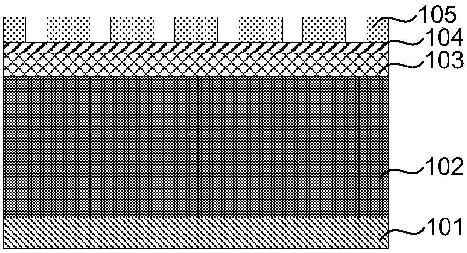
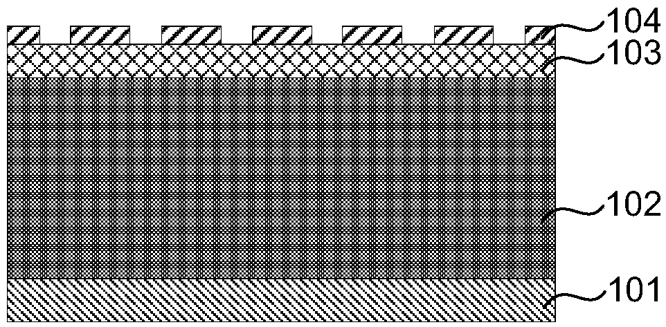
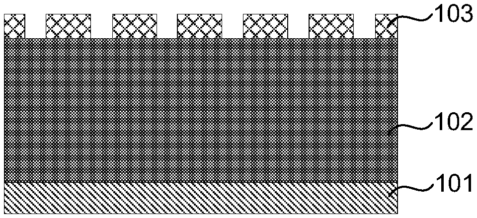
[0038] image 3 is a process flow diagram of the hole forming method according to the embodiment of the present invention. 4(A) to 4(J) show cross-sectional views at different stages of the hole forming method according to the embodiment of the present invention.

[0039] The hole forming method of the present embodiment generally includes the following steps:

[0040] S1: providing a substrate and a layer to be etched arranged on the substrate;

[0041] S2: forming a first etching material layer on the layer to be etched;

[0042] S3: Etching the first etching material layer to form a first mask layer;

[0043] S4: forming an auxiliary mask layer in the gap of the first mask layer; and

[0044] S5: Etching the layer to be etched by using the first mask layer and the auxiliary mask layer as masks to form holes.

[0045] Specifically, in step S1, for example as shown in FIG. 4(A), a substrate 101 is provided, and a layer 102 to be etched is formed on the substrate 101.

...


PUM


Abstract

The invention provides a hole forming method. The hole forming method comprises the steps of providing a substrate and a to-be-etched layer arranged on the substrate; and forming a first etching material layer on the to-be-etched layer; performing etching on the first etching material layer to form a first mask layer; forming an auxiliary mask layer in a gap of the first mask layer; and etching the to-be-etched layer by taking the first mask layer and the auxiliary mask layer as masks to form holes. By adopting the auxiliary mask layer, the requirements of each step on equipment and process can be reduced, and the appearance of the structure obtained in each step can be conveniently controlled, so that the finally formed hole has high morphology features, and a situation that the size of the bottom and the size of the top of the reference case have a large difference can be avoided; and in addition, the condition that the aperture roundness of each hole is not consistent can be improved.

Description

technical field [0001] The invention relates to a method for forming a hole in a semiconductor manufacturing process, in particular to a method for forming a deep hole on a hard mask in a three-dimensional memory. Background technique [0002] With the development of planar flash memory, the production process of semiconductors has made great progress. However, in recent years, the development of planar flash memory has encountered various challenges: physical limits, existing development technology limits, and storage electron density limits. In this context, in order to solve the difficulties encountered in planar flash memory and to seek lower production costs per unit storage unit, various three-dimensional memory structures emerged as the times require, and solve the problem of 2D or planar NAND by stacking memory particles together. Limitations imposed by flash memory. Contents of the invention [0003] The technical problem to be solved by the invention [0004] ...

Claims


Application Information

Patent Timeline
IPC IPC(8): H01L21/033H01L27/115H01L27/11556H01L27/11582
CPCH01L21/0337H10B41/27H10B69/00H10B43/27
Inventor 向银松王猛揭黎肖为引黄竹青黄海辉李飞
Owner YANGTZE MEMORY TECH CO LTD
Why Eureka
Try Eureka