Pixel circuit and driving method thereof, display panel and display device

A technology for pixel circuits and driving modules, applied in static indicators, instruments, etc., can solve the problems of exciton quenching, voltage increase, OLED luminous efficiency and life decay rate acceleration, etc., to avoid ion aggregation, luminous efficiency and use. Life-enhancing effect

Inactive Publication Date: 2018-11-23
BOE TECH GRP CO LTD +1
View PDF8 Cites 21 Cited by
  • Summary
  • Abstract
  • Description
  • Claims
  • Application Information

AI Technical Summary

Problems solved by technology

[0003] In the prior art, in the process of driving the OLED to emit light, it is necessary to apply a forward bias voltage to the OLED to drive the OLED to emit light, so that the OLED is always in a bias state, resulting in ion aggregation inside the OLED, forming a built-in electric field To offset the external bias, the voltage will increase with time; and the ion aggregation inside the OLED will easily lead to the quenching of the excitons, thus accelerating the luminous efficiency and life decay rate of the OLED

Method used


Image

  • Pixel circuit and driving method thereof, display panel and display device
  • Pixel circuit and driving method thereof, display panel and display device
  • Pixel circuit and driving method thereof, display panel and display device

Examples


Embodiment 1

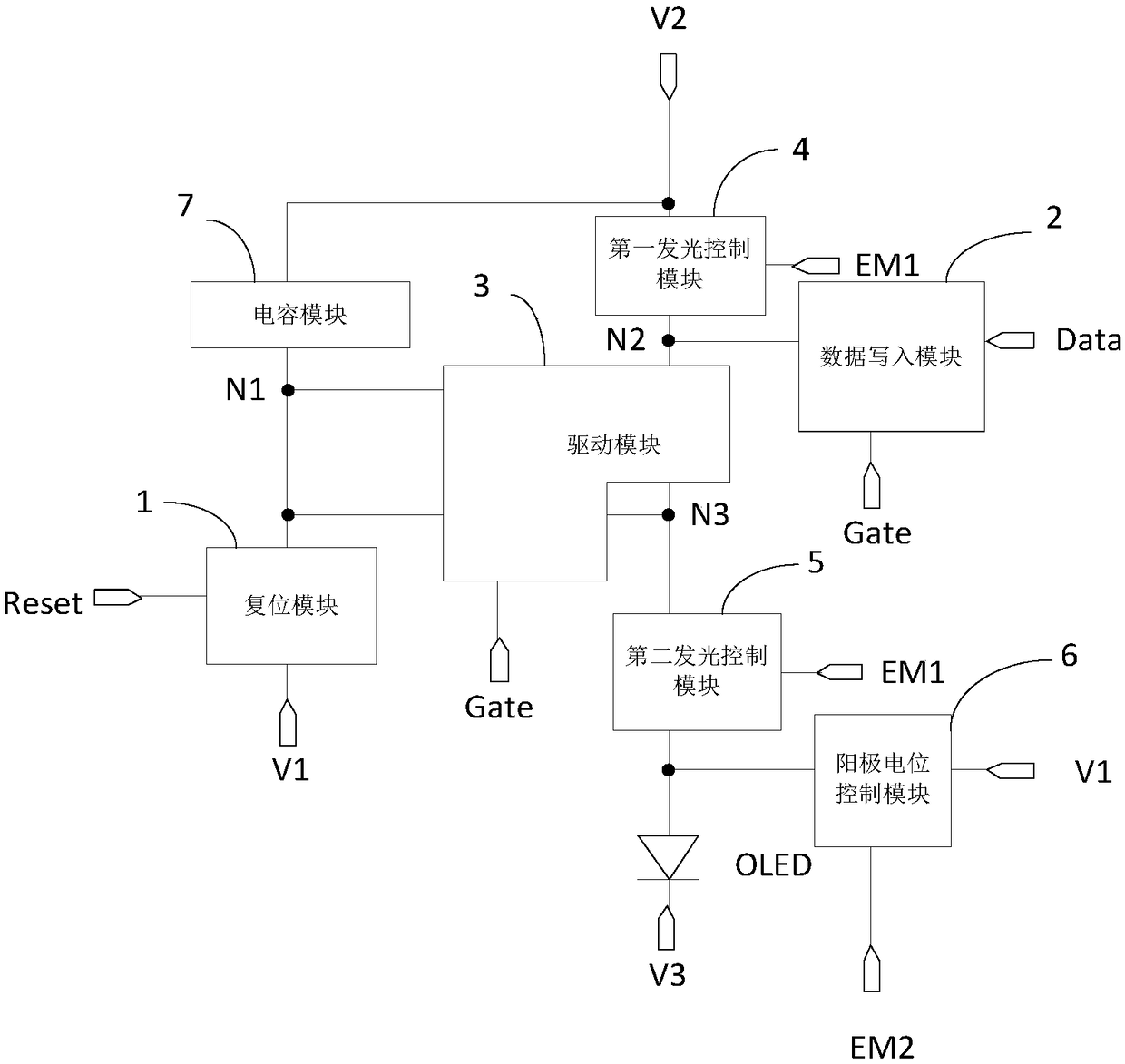
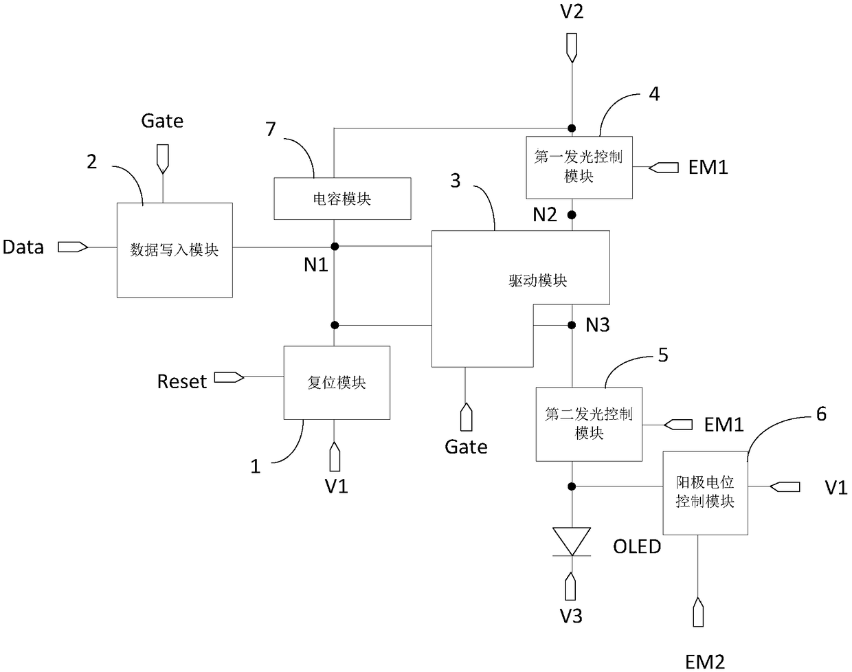
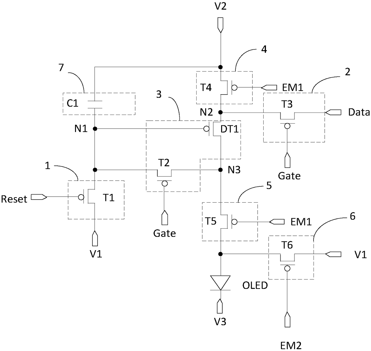
[0108] Specifically, choose the Figure 5 The three stages t1, t2 and t3 in the input timing diagram are shown.

[0109] In the t1 stage, Reset=0, Gate=1, EM1=1, Data=0, EM2=0.

[0110] Since Reset=0, the first transistor T1 is in a conduction state, and the signal of the first voltage signal terminal V1 is provided to the first node N1 to reset the potential of the first node N1; since EM2=0, the sixth transistor T6 Turning on provides the signal of the first voltage signal terminal V1 to the anode of the light emitting device OLED, and resets the potential of the anode of the light emitting device OLED.

[0111] In the t2 stage, Reset=1, Gate=0, EM1=1, Data=1, EM2=0.

[0112] Since Gate=0, the second transistor T2 and the third transistor T3 are turned on, the second transistor T2 is turned on to provide the potential of the first node N1 to the third node N3, and the third transistor T3 is turned on to provide the data of the data signal terminal Data The signal Vdata is...

Embodiment 2

[0118] Specifically, choose the Figure 6 The three stages t1, t2 and t3 in the input timing diagram are shown.

[0119] The difference between the three stages of this embodiment and the first embodiment is that the duty cycle of the control signal sent by the first control terminal EM1 in the t3 stage is smaller than that of the control signal sent by the first control terminal EM1 in the t3 stage of the embodiment. Duty cycle, by adjusting the duty cycle of the control signal sent by the first control terminal EM1 to reduce the light emitting time of the light emitting device OLED, so as to achieve the purpose of adjusting the brightness of the light emitting device OLED. Since the phase of the signal of the second control terminal EM2 is always opposite to that of the signal of the first control terminal EM1, the duty cycle of the signal of the second control terminal EM2 follows the duty cycle of the signal of the first control terminal EM1. Corresponding adjustments are...


PUM


Abstract

The present invention discloses a pixel circuit and a driving method thereof, a display panel and a display device. The pixel circuit comprises a reset module, a data writing-in module, a drive module, a first light-emitting control module, a second light-emitting control module, an anode potential control module, a capacitive module and a light-emitting device. Through cooperative work of the modules mentioned above, the pixel circuit drives the light-emitting device to emit light, and the second light-emitting control module supplies a voltage of an output end of the drive module to an anodeof the light-emitting device in a light-emitting stage; and the anode potential control module supplies signals of a first voltage signal terminal to the anode of the light-emitting device in a non-light-emitting stage to allow the bias voltage of the light-emitting device in the non-light-emitting stage to be opposite to the bias voltage of the light-emitting device in the light-emitting stage so as to improve the light-emitting efficiency and the service life of the light-emitting device.

Description

technical field [0001] The present invention relates to the field of display technology, in particular to a pixel circuit and a driving method thereof, a display panel and a display device. Background technique [0002] Organic Light Emitting Diode (OLED) is one of the hot spots in the field of display research today. Compared with Liquid Crystal Display (LCD), OLED has low energy consumption, low production cost, self-illumination, wide viewing angle and response At present, OLED displays have begun to replace traditional LCD displays in display fields such as mobile phones, PDAs, and digital cameras. Among them, pixel circuit design is the core technical content of OLED display, which has important research significance. [0003] In the prior art, in the process of driving the OLED to emit light, it is necessary to apply a forward bias voltage to the OLED to drive the OLED to emit light, so that the OLED is always in a bias state, resulting in ion aggregation inside the O...

Claims


Application Information

Patent Timeline
Patent Type & Authority Applications(China)
IPC IPC(8): G09G3/3258G09G3/3266G09G3/3208
CPCG09G3/3208G09G3/3258G09G3/3266G09G2300/0452G09G2320/045G09G3/3233G09G2310/061G09G2230/00G09G2310/06G09G2300/0861
Inventor 黎倩张兵
Owner BOE TECH GRP CO LTD
Why Eureka
Try Eureka