Wafer inspection system and wafer inspection method

A detection system and chip technology, applied in semiconductor/solid-state device testing/measurement, electrical components, semiconductor/solid-state device manufacturing, etc. spot, detection results are accurate

Active Publication Date: 2018-11-23
BEIJING NAURA MICROELECTRONICS EQUIP CO LTD
View PDF8 Cites 0 Cited by
  • Summary
  • Abstract
  • Description
  • Claims
  • Application Information

AI Technical Summary

Problems solved by technology

[0005] However, the wafer detection system with the above structure will cause the defect of poor wafer recognition due to the differences in reflectivity, size and flatness of different wafers.
[0006] In addition, when the manipulator passes the sensor, if the sensor is a specular reflection sensor, it needs to be strictly aligned so that the reflected light can be accurately absorbed into the receiver. If the sensor is slightly displaced, the reflected light may not be accurately reflected to the receiver, which may easily cause failure , In addition, if the surface of the wafer is dark and the reflectivity is not enough, the wafer cannot be detected
[0007] Finally, when the manipulator passes the sensor, if the diffuse reflection sensor is used, it also uses the principle of reflection. Therefore, if the size or shape of the wafer does not match the predetermined one, it will also report an error, and it is impossible to accurately calculate the wafer through the duration of the light sensitivity change. Coordinate position on the machine

Method used


Image

  • Wafer inspection system and wafer inspection method
  • Wafer inspection system and wafer inspection method
  • Wafer inspection system and wafer inspection method

Examples


Embodiment Construction

[0057] Specific embodiments of the present invention will be described in detail below in conjunction with the accompanying drawings. It should be understood that the specific embodiments described here are only used to illustrate and explain the present invention, and are not intended to limit the present invention.

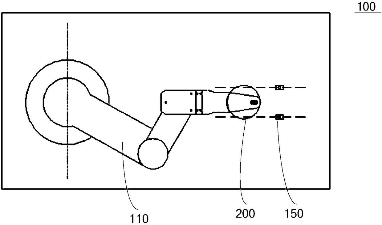
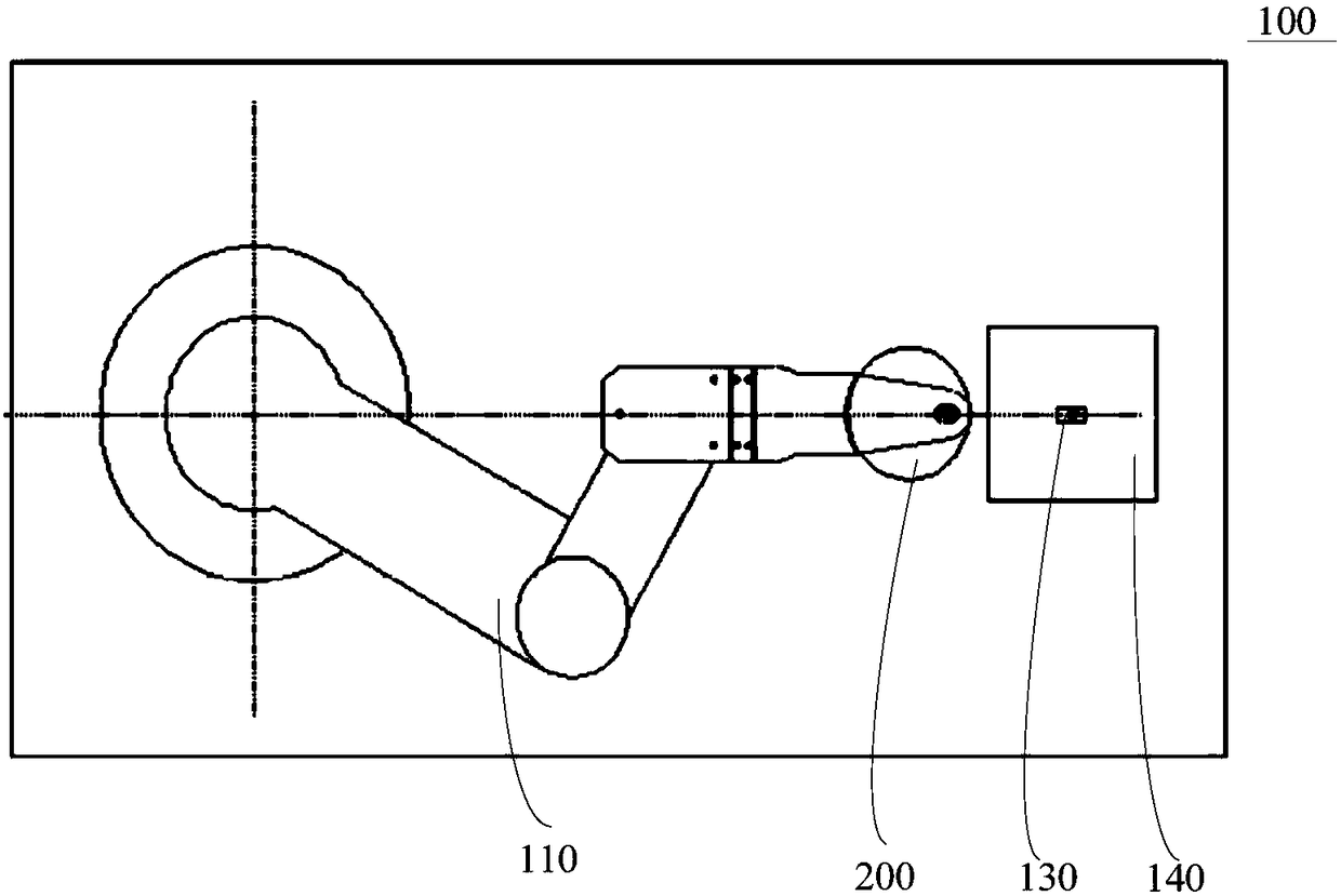
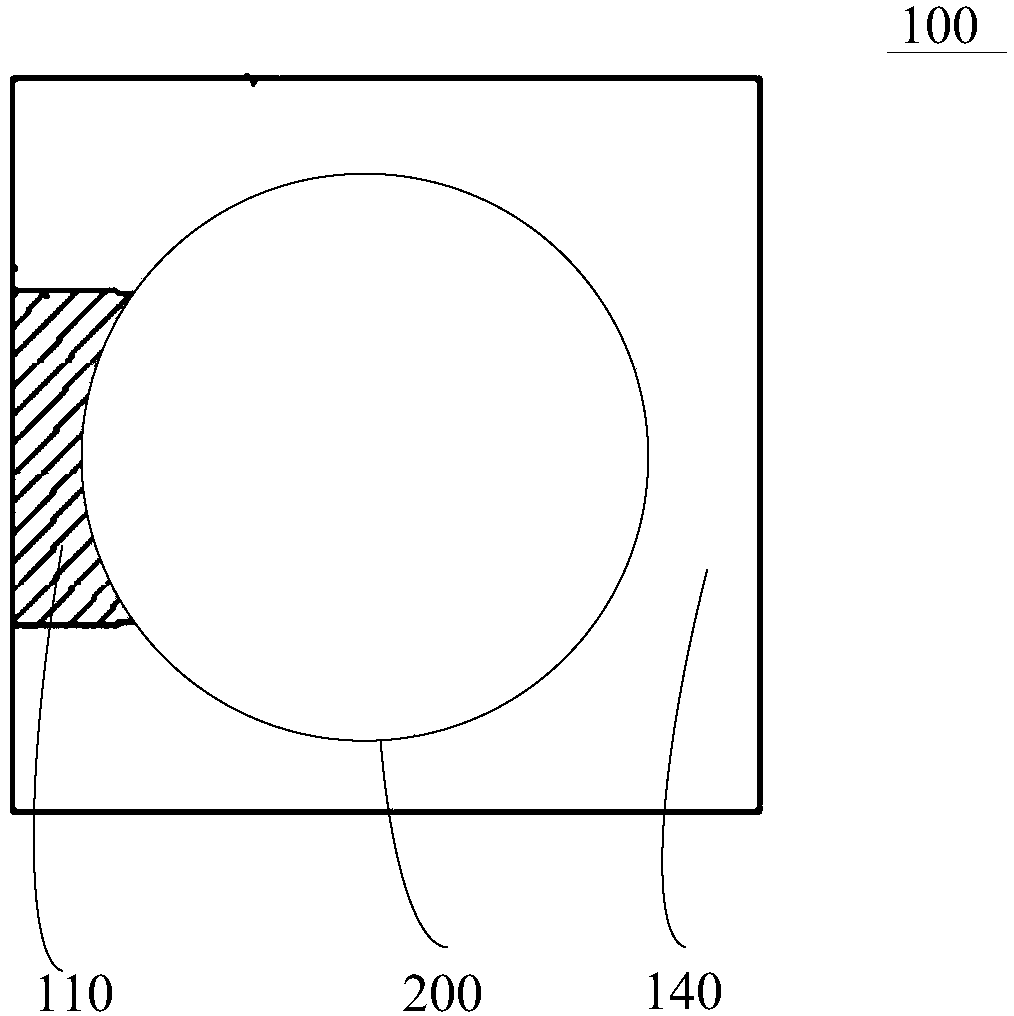
[0058] refer to Figure 2 to Figure 6 , the first aspect of the present invention relates to a wafer inspection system 100 . The wafer detection system 100 includes a manipulator 110, which is mainly used to transport the wafer 200. For example, in the PVD process production process, the wafer 200 often needs to be transferred back and forth between different reaction chambers. At this time, the manipulator 110 can be used. The wafer 200 is transported to different stations according to a predetermined track, so that the wafer 200 is processed accordingly at the station.

[0059] When the manipulator 110 moves to a preset image acquisition position, for exampl...


PUM


Abstract

The invention discloses a wafer inspection system and a wafer inspection method. The wafer inspection system comprises a manipulator, a controller and a polarization camera, the manipulator is used for acquiring and transmitting a wafer, and the manipulator sends out an image acquisition signal when the manipulator moves to a preset image acquisition position; the controller is used for receivingthe image acquisition signal and sending out an image generation signal; the polarization camera is used for receiving and executing the image generation signal, so as to photograph an image of the wafer; and the controller is also used for receiving the image of the wafer, matching the image of the wafer with a preset reference image and judging an existential state of the wafer on the manipulator on the basis of a matching result. The wafer inspection system of a structure of the embodiment of the invention acquires the image of the wafer at the preset image acquisition position by utilizingthe polarization camera and can avoid the hot spot problem, caused by relatively high reflectance, of most wafers, thus an inspection result is more accurate.

Description

technical field [0001] The invention relates to the technical field of semiconductors, in particular to a wafer detection system and a wafer detection method. Background technique [0002] Generally, physical vapor deposition (Physical Vapor Deposition, PVD) refers to the process of using physical processes to realize material transfer, and transfer atoms or molecules from the source to the surface of the substrate. Its function is to spray some particles with special properties (high strength, wear resistance, heat dissipation, corrosion resistance, etc.) on the matrix with lower performance, so that the matrix has better performance. Common PVD basic methods include vacuum evaporation, sputtering, and ion plating (hollow cathode ion plating, hot cathode ion plating, arc ion plating, active reactive ion plating, radio frequency ion plating, and DC discharge ion plating). [0003] In the production process of PVD process, wafers are transferred back and forth between differ...

Claims


Application Information

Patent Timeline
IPC IPC(8): H01L21/67H01L21/66
CPCH01L21/67259H01L22/12
Inventor 徐义
Owner BEIJING NAURA MICROELECTRONICS EQUIP CO LTD
Why Eureka
Try Eureka