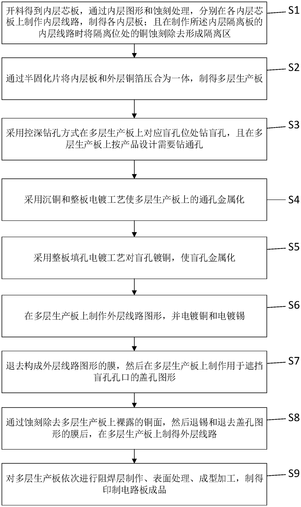
Printed circuit board with blind hole instead of back drill hole and manufacturing method thereof
A technology of printed circuit board and manufacturing method, which is applied in the direction of printed circuit manufacturing, printed circuit, and electrical connection formation of printed components, etc., which can solve the problems of easy plugging of back-drilled holes, etc., and achieve the effect of simple structure and avoiding short circuit
- Summary
- Abstract
- Description
- Claims
- Application Information
AI Technical Summary
Problems solved by technology
Method used
Image

Examples
Embodiment 1
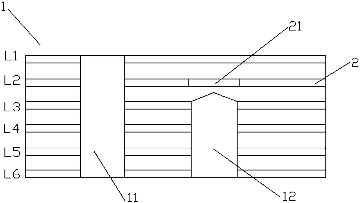
[0030] combine figure 1 and figure 2 As shown, this embodiment provides a method for manufacturing a printed circuit board with blind holes instead of back-drilled holes. The printed circuit board 1 is provided with blind holes 12, which constitute the inner layer of the printed circuit board. The area on the inner board used to make blind holes is called the blind hole position, and the inner board adjacent to the bottom of the 12-hole blind hole is called the inner layer isolation board 2, and the inner layer isolation board 2 is connected to the bottom of the 12-hole blind hole. The adjacent side and the area opposite to the bottom of the blind hole 12 are called isolation positions; in the present embodiment, as figure 2 As shown, the layers L3-L6 are laminates that need to be connected, and there are blind holes 12 on the layers L3-L6, and the layer L2 is the inner layer isolation board 2;
[0031] Described preparation method comprises the following steps:
[0032] ...
Embodiment 2
[0044] Such as figure 2 As shown, this embodiment provides a printed circuit board with blind holes instead of back-drilled holes, and the multiple laminates that need to be connected to the printed circuit board are connected through electroplated blind holes 12, and the blind holes 12 are connected to each other. The inner layer board adjacent to the bottom is called the inner layer isolation board 2, and the copper at the side adjacent to the bottom of the blind hole 12 and the area opposite to the bottom of the blind hole 12 is etched away to form an isolation board. Zone 21; in this embodiment, as figure 2 As shown, the layers L3-L6 are laminates to be connected, the layers L3-L6 are provided with blind holes 12 , and the layer L2 is the inner isolation board 2 .
[0045] Specifically, the depth of the blind hole 12 is smaller than the distance from the isolation hole 21 to the opening end of the blind hole 12, that is, the distance from L2 to L6, so that even if the i...
PUM
 Abstract
Description
Claims
Application Information