Organic light emitting apparatus and organic light emitting device
An electroluminescent device and electroluminescent device technology, which are applied in the direction of electro-solid devices, electrical components, semiconductor devices, etc., can solve the problems of being easily lit at the same time, low gray-scale color shift, etc., so as to improve display quality and reduce The effect of injecting potential barrier and reducing energy level difference
- Summary
- Abstract
- Description
- Claims
- Application Information
AI Technical Summary
Problems solved by technology
Method used
Image

Examples
Embodiment 1
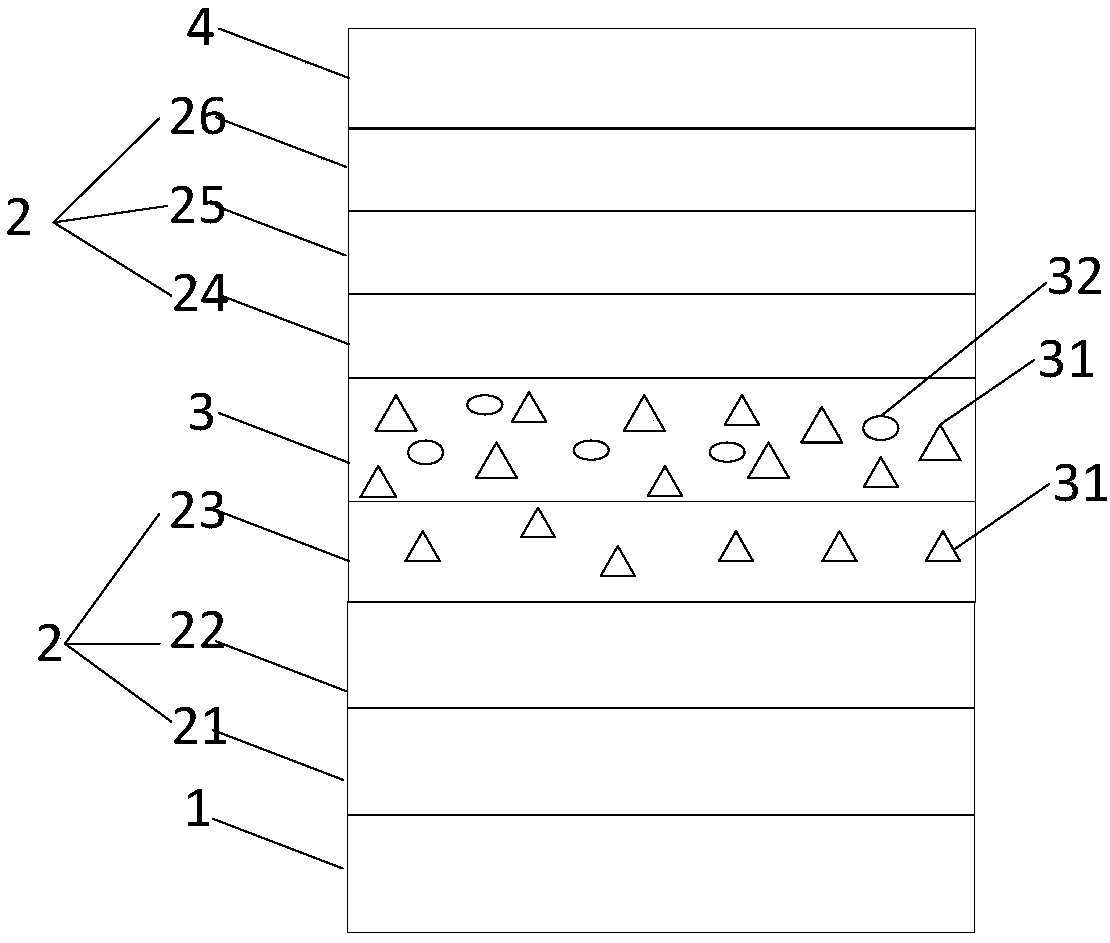
[0041] An embodiment of the present invention provides an organic electroluminescent device, such as figure 2 As shown, it includes a first electrode layer 1 , a carrier functional layer 2 , a light emitting layer 3 and a second electrode layer 4 which are stacked. The first electrode layer 1 is an anode, and the second electrode layer 4 is a cathode; or the first electrode layer 1 is a cathode, and the second electrode layer 4 is an anode. In the following, the first electrode layer 1 is used as an anode, and the second electrode layer 4 is used as a cathode as an example for illustration. The carrier functional layer 2 has one or more layers and is disposed between the light emitting layer 3 and the first electrode layer 1 and / or between the light emitting layer 3 and the second electrode layer 4 .
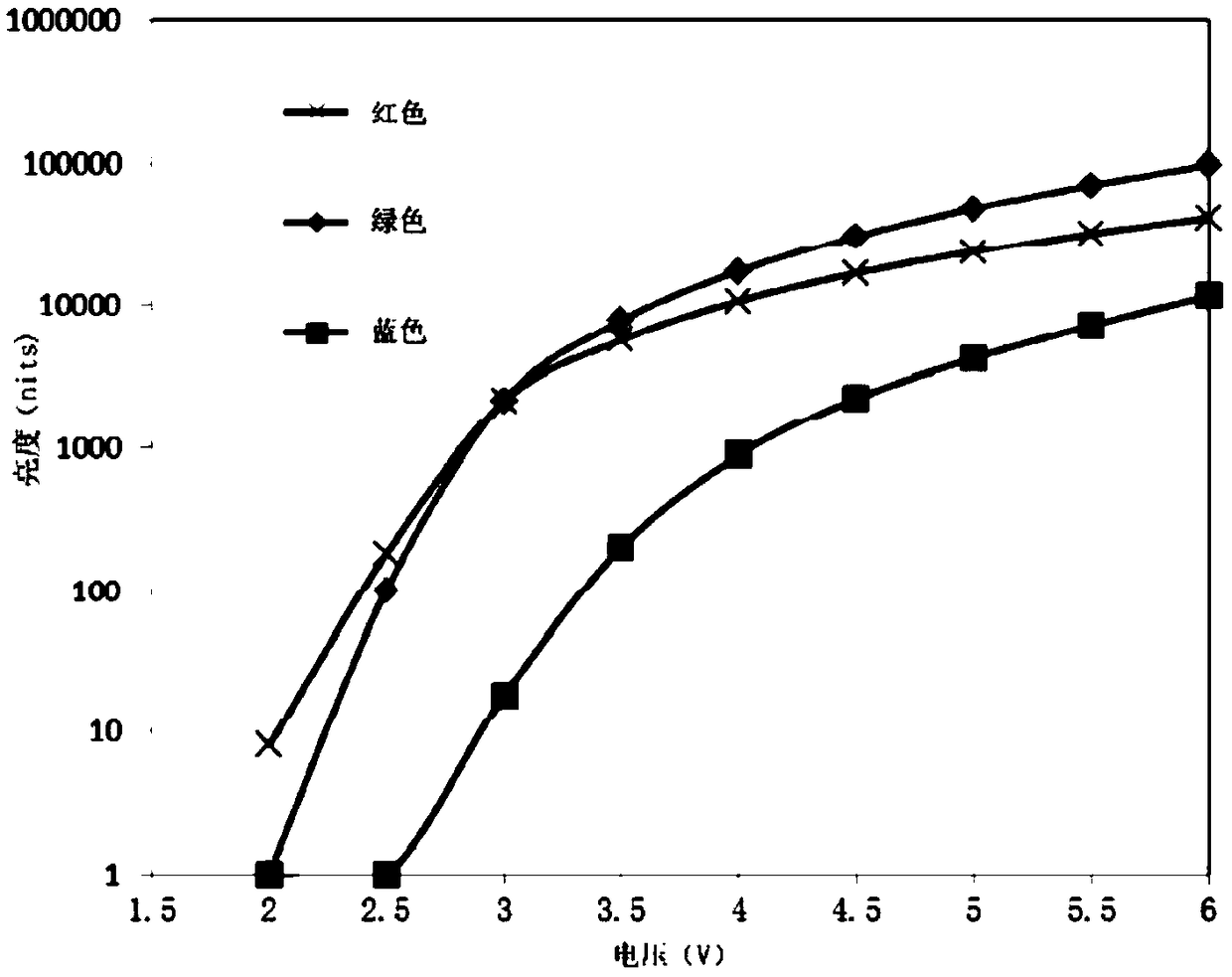
[0042] In the prior art, the process of lighting an organic electroluminescent device is to apply a certain driving voltage to the first electrode layer 1 and the second elect...
Embodiment 2
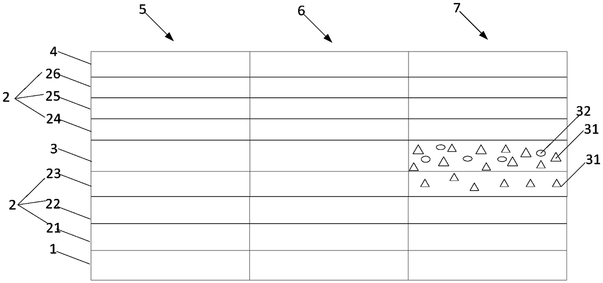
[0060] An embodiment of the present invention provides an organic electroluminescent device, including several pixel units distributed in an array, such as image 3 As shown, each pixel unit includes a red light sub-pixel unit 5 , a green light sub-pixel unit 6 and a blue light sub-pixel unit 7 .
[0061] Each sub-pixel unit includes a stacked first electrode layer 1, a carrier functional layer 2, a light-emitting layer 3, and a second electrode layer 4, a red sub-pixel unit 5, a green sub-pixel unit 6, and a blue sub-pixel unit 7 The light emitting layers 3 in the figure are red light emitting layer, green light emitting layer and blue light emitting layer respectively.
[0062] At least one carrier functional layer 2 close to the blue light emitting layer in the blue light sub-pixel unit 7 is doped with materials in the blue light emitting layer.
[0063] For specific content, reference may be made to the description in Embodiment 1, and details are not repeated here.
[0...
Embodiment 3
[0070] The embodiment of the present invention provides a specific organic electroluminescence device, including several pixel units distributed in an array, and each pixel unit includes a red sub-pixel unit 5 , a green sub-pixel unit 6 and a blue sub-pixel unit 7 .
[0071] Each sub-pixel unit includes a first electrode layer 1 (anode), a carrier functional layer 2 (hole injection layer 21, a hole transport layer 22, an electron blocking layer 23), a light-emitting layer 3, a carrier Flow sub-pixel unit 5, green sub-pixel unit 6 and blue sub-pixel unit 7 The light-emitting layers 3 are respectively a red light-emitting layer, a green light-emitting layer and a blue light-emitting layer.
[0072] Wherein, the blue light-emitting layer 3 includes a host material CBP and a guest material BCzVBI, and the electron blocking layer 23 in the blue sub-pixel unit 7 is doped with the host material CBP in the blue light-emitting layer, and the doping ratio is 25 wt%. The electron blocki...
PUM
| Property | Measurement | Unit |
|---|---|---|
| Thickness | aaaaa | aaaaa |
| Thickness | aaaaa | aaaaa |
| Thickness | aaaaa | aaaaa |
Abstract
Description
Claims
Application Information
 - R&D
- Intellectual Property
- Life Sciences
- Materials
- Tech Scout
- Unparalleled Data Quality
- Higher Quality Content
- 60% Fewer Hallucinations
Browse by: Latest US Patents, China's latest patents, Technical Efficacy Thesaurus, Application Domain, Technology Topic, Popular Technical Reports.
© 2025 PatSnap. All rights reserved.Legal|Privacy policy|Modern Slavery Act Transparency Statement|Sitemap|About US| Contact US: help@patsnap.com