Organic light emitting device

An electroluminescence device and luminescence technology, applied in the direction of circuits, electrical components, electric solid-state devices, etc., can solve the problems of low luminance and color shift of red photon sub-pixels and green photon sub-pixels, achieve good transmission performance, and improve low gray Color gradients, reducing the effect of lateral migration

Active Publication Date: 2018-12-07
YUNGU GUAN TECH CO LTD
View PDF13 Cites 4 Cited by
  • Summary
  • Abstract
  • Description
  • Claims
  • Application Information

AI Technical Summary

Problems solved by technology

In practical applications, when the blue sub-pixel is turned on, although the voltage is mainly across the blue sub-pixel, due to the better conductivity of the common hole injection layer, part of the voltage will be applied to the green sub-pixel through the common hole injection layer. In the photo-sub-pixel and / or the red-light sub-pixel, since the turn-on voltages of the red-light sub-pixel and the green-light sub-pixel are both lower than the turn-on voltage of the blue-light sub-pixel, the red-light sub-pixel and / or the green-light sub-pixel are easy to be turned on simultaneously
That is, in the case of low gray scale, the luminous brightness of the red sub-pixel and / or green sub-pixel cannot strictly meet the requirements to achieve the low-brightness display effect, and the low gray scale color cast (reddish) phenomenon occurs

Method used


Image

  • Organic light emitting device
  • Organic light emitting device
  • Organic light emitting device

Examples


Embodiment 1

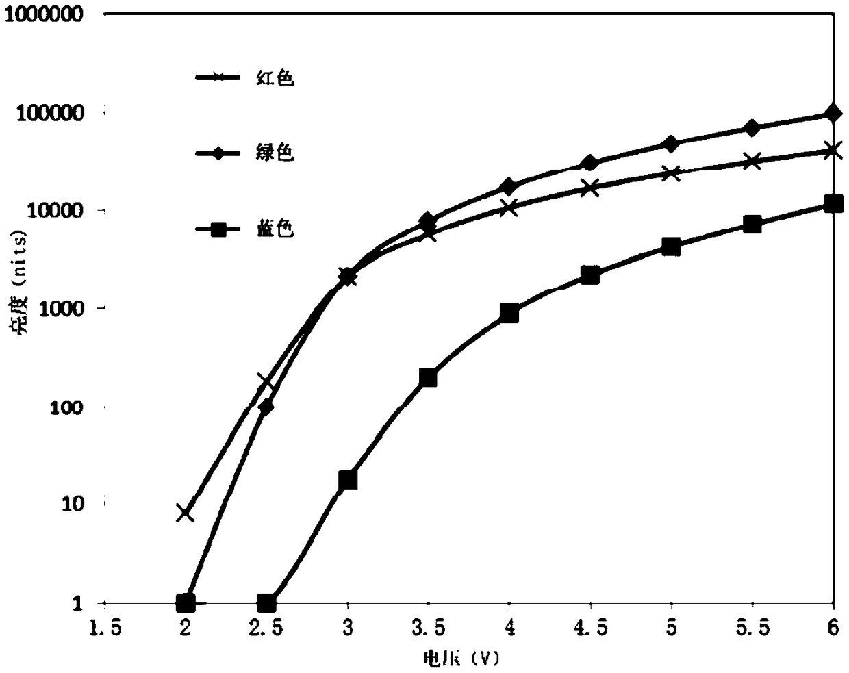
[0067] This embodiment provides a specific example of an organic electroluminescence device, which includes several pixel units distributed in an array, and the pixel units include a red sub-pixel unit 1R, a green sub-pixel unit 1G and a blue sub-pixel unit 1B.

[0068] The red sub-pixel unit 1R includes an anode, a hole injection layer, a light-emitting layer 13, an electron injection layer, and a cathode that are stacked in sequence, and the green sub-pixel unit 1G includes an anode, a hole injection layer, a light-emitting layer 13, and an electron injection layer that are stacked in sequence. layer and cathode, the blue light sub-pixel unit 1B includes an anode, a hole injection layer, a light emitting layer 13 , an electron injection layer and a cathode which are stacked in sequence.

[0069] Among them, the hole injection layer of each sub-pixel unit is made of a compound with a planar molecular structure stacked along the direction perpendicular to the light-emitting lay...

Embodiment 2

[0074] This embodiment provides an organic electroluminescent device, which is basically the same as the organic electroluminescent device described in Example 1, the only difference being:

[0075] The hole injection layers of the red light sub-pixel unit 1R and the green light sub-pixel unit 1G are stacked in the direction perpendicular to the light-emitting layer 13 by using a compound with a planar molecular structure, and are staggered in a direction parallel to the light-emitting layer 13. The specific molecular structure compound is (TIPS-Pentacene).

[0076] The device structure of the red sub-pixel unit 1R in this embodiment is: ITO(10nm) / Ag(100nm) / ITO(10nm) / TIPS-Pentacene(10nm) / TPD(200nm) / CBP:Ir(piq) 3 (3%, 30nm) / TPBi(40nm) / LiF(1nm) / Mg:Ag(20%, 15nm) / NPB(60nm).

[0077] The device structure of the green sub-pixel unit 1G in this embodiment is: ITO(10nm) / Ag(100nm) / ITO(10nm) / TIPS-Pentacene(10nm) / TPD(160nm) / CBP:Ir(ppy) 3 (3%, 30nm) / TPBi(40nm) / LiF(1nm) / Mg:Ag(20%, 15nm) / ...

Embodiment 3

[0080] This embodiment provides an organic electroluminescent device, which is basically the same as the organic electroluminescent device described in Example 1, the only difference being:

[0081] Specifically, the compound having a planar molecular structure in each sub-pixel unit is: iron phthalocyanine (abbreviation: FePc).

[0082] The device structure of the red sub-pixel unit 1R in this embodiment is: ITO(10nm) / Ag(100nm) / ITO(10nm) / FePc(10nm) / TPD(200nm) / CBP:Ir(piq) 3 (3%, 30nm) / TPBi(40nm) / LiF(1nm) / Mg:Ag(20%, 15nm) / NPB(60nm).

[0083] The device structure of the green sub-pixel unit 1G in this embodiment is: ITO(10nm) / Ag(100nm) / ITO(10nm) / FePc(10nm) / TPD(160nm) / CBP:Ir(ppy) 3 (3%, 30nm) / TPBi(40nm) / LiF(1nm) / Mg:Ag(20%, 15nm) / NPB(60nm).

[0084] The device structure of the blue light sub-pixel unit 1B in this embodiment is: ITO (10nm) / Ag (100nm) / ITO (10nm) / FePc (10nm) / TPD (120nm) / CBP: Firpic (3%, 30nm) / TPBi (40nm) / LiF(1nm) / Mg:Ag(20%, 15nm) / NPB(60nm).


PUM


Abstract

The invention discloses an organic light emitting device which comprises sub pixel units in a plurality of light emitting colors. Each sub pixel unit includes a first electrode layer, a carrier function layer, a light emitting layer and a second electrode layer which are stacked together. Each carrier function layer at least includes a carrier injection layer. The carrier injection layer in the sub pixel unit in at least one light emitting color is formed by stacking compounds with a planar molecular structure in the direction parallel to the light emitting layer. The compounds with a planar molecular structure are arranged in a staggered manner in the direction parallel to the light emitting layer. The carriers in each carrier function layer migrate along the molecule stacking direction.The carrier injection layers which are formed by stacking compounds with a planar molecular structure in the direction parallel to the light emitting layer and arranging the compounds in a staggered manner in a direction parallel to the light emitting layer reduce the transverse migration of carriers, improve the problem that the adjacent sub pixel unit is lighted up due to carrier migration whena single sub pixel unit is lighted up, and improve the low-grayscale color deviation.

Description

technical field [0001] The invention belongs to the field of display technology, and in particular relates to an organic electroluminescent device. Background technique [0002] Organic electroluminescent display (English full name Organic Light Emitting Display, referred to as OLED) is an active light emitting display device, because it has the advantages of simple preparation process, low cost, high contrast, wide viewing angle, low power consumption, etc. Large-screen display, easy to match with integrated circuit drivers, easy to realize flexible display and other advantages, is expected to become the mainstream flat panel display technology of the next generation, and is one of the most concerned technologies in flat panel display technology at present. [0003] figure 1 The voltage-brightness curves of the RGB three-color sub-pixels in the existing full-color display device are shown. It can be seen from the figure that in the existing OLED display device, the turn-o...

Claims


Application Information

Patent Timeline
IPC IPC(8): H01L51/54H01L51/50
CPCH10K85/615H10K85/654H10K85/6572H10K50/11H10K2101/10H10K50/17
Inventor 周小康李梦真何麟李维维刘彬杨鹤
Owner YUNGU GUAN TECH CO LTD
Why Eureka
Try Eureka