A preparation method of a nanoporous gold film and a silicon substrate using the film

A manufacturing method and nanopore technology, which are applied in the manufacture of microstructure devices, metal material coating processes, processes for producing decorative surface effects, etc. Raman Spectroscopy Characterization Weak Issues

Inactive Publication Date: 2018-12-14
纤瑟(天津)新材料科技有限公司
View PDF6 Cites 6 Cited by
  • Summary
  • Abstract
  • Description
  • Claims
  • Application Information

AI Technical Summary

Problems solved by technology

However, both nanoporous gold nuggets and nanoporous gold films have defects

Method used


Image

  • A preparation method of a nanoporous gold film and a silicon substrate using the film
  • A preparation method of a nanoporous gold film and a silicon substrate using the film
  • A preparation method of a nanoporous gold film and a silicon substrate using the film

Examples


Embodiment Construction

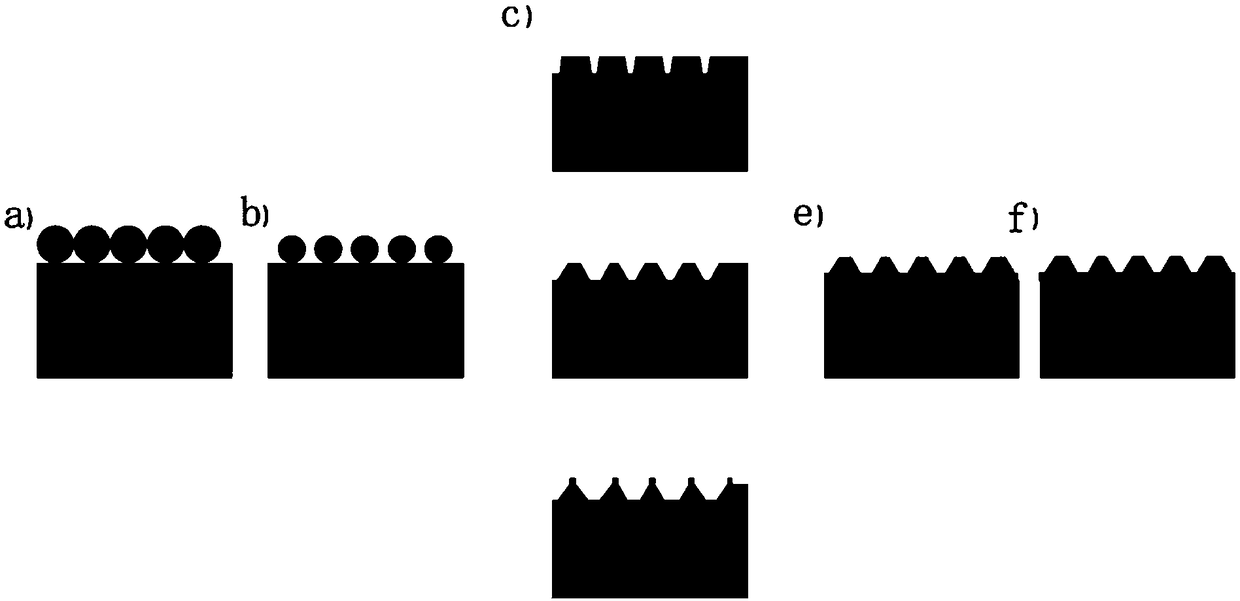
[0027] The present invention is specifically described below in conjunction with accompanying drawing, as Figure 1-2 Shown, a kind of preparation method of nanoporous gold thin film and the silicon base that uses this thin film, comprise the silicon chip to be processed, the preparation method of microstructure nanoporous gold thin film comprises the following steps:

[0028] a. A uniform single-layer polystyrene microsphere layer is formed on the surface of the silicon wafer, and the single-layer polystyrene microsphere layer is used to protect the surface of the silicon wafer where the microsphere layer is located from being affected by the etching gas.

[0029] b. Use oxygen plasma to reduce the diameter of polystyrene microspheres to ensure the microsphere gap. The size of the microsphere gap directly affects the microstructure etched on the subsequent silicon wafer.

[0030] c. Etching microstructures on the silicon wafer, and etching different microstructures by control...


PUM


Abstract

The invention discloses a preparation method of a nanoporous gold film and a silicon substrate using the film, includes silicon wafers to be processed. A method for fabricate a microstructured nanoporous gold film comprise that following steps of: forming a uniform monolayer polystyrene microsphere layer on the surface of the silicon wafer, oxygen plasma being used to reduce the diameter of polystyrene microspheres and ensure the gap between microspheres, etching the microstructure on the silicon wafer, removing the polystyrene microspheres layer from the processing surface of the silicon wafer to form silicon substrate, uniformly covering the surface of the silicon substrate with a layer of gold-silver alloy film, removing the silver atoms in the gold-silver alloy film, and forming the microstructure nanoporous gold film. The invention has the beneficial effect that, by forming polystyrene microspheres on the surface of silicon wafer and etching different silicon surface microstructures on the surface of silicon wafer by reactive ion etching, the porous gold thin films were laid on the surface of silicon wafer with different microstructures, and the optimal porous gold thin filmstructure for Raman spectroscopy measurement could be obtained by comparison.

Description

technical field [0001] The invention relates to the field of semiconductors, in particular to a manufacturing method of a nanoporous gold thin film and a silicon base using the thin film. Background technique [0002] Surface plasmonic metal nanoparticles have great potential in the fields of sensing, photovoltaics, imaging, and biomedicine. Among them, sponge-like gold (nanoporous gold) materials with nanovoids have attracted extensive attention because of their unique three-dimensional bicontinuous nanostructures. However, both nanoporous gold nuggets and nanoporous gold films have defects such as untunable properties and weak surface Raman spectrum characterization. Contents of the invention [0003] The purpose of the present invention is in order to solve the above-mentioned problem, has designed a kind of preparation method of nanoporous gold thin film and the silicon base that uses this thin film. [0004] Achieving the above-mentioned purpose The technical scheme...

Claims


Application Information

Patent Timeline
IPC IPC(8): B81C1/00
CPCB81C1/00349B81C1/00373
Inventor 赵复生李静婷赵俊洋
Owner 纤瑟(天津)新材料科技有限公司
Why Eureka
Try Eureka