Analog signal FFT implementation method based on FPGA and circuit thereof

A technology of analog signal and implementation method, which is applied in the field of spectrum analysis of signal processing, can solve the problems such as the effect is not intuitive enough, and achieve the effect of convenient capture and analysis, fast speed and good real-time response

Inactive Publication Date: 2018-12-14
ZHEJIANG WANLI UNIV
View PDF4 Cites 7 Cited by
  • Summary
  • Abstract
  • Description
  • Claims
  • Application Information

AI Technical Summary

Problems solved by technology

This method needs to generate more complex control timing, but it has good real-time performance, it is convenient to modify the number of FFT points, and it has strong portability. However, this method only mentions the use of IP cores for operations in conventional designs, but it is specific for analog sampling signals from the beginning. It is not mentioned until the realization of FFT transformation. At the same time, in the conventional design, the result of FFT transformation is usually calculated by MATLAB, and the effect is not intuitive enough.

Method used


Image

  • Analog signal FFT implementation method based on FPGA and circuit thereof
  • Analog signal FFT implementation method based on FPGA and circuit thereof
  • Analog signal FFT implementation method based on FPGA and circuit thereof

Examples


Embodiment 1

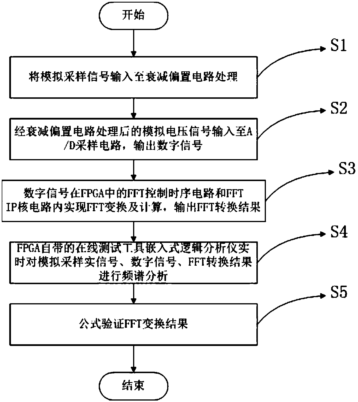
[0048] like figure 1 As shown, the present embodiment relates to a FFT implementation method of an FPGA-based analog signal, and the FFT implementation method includes the following steps:

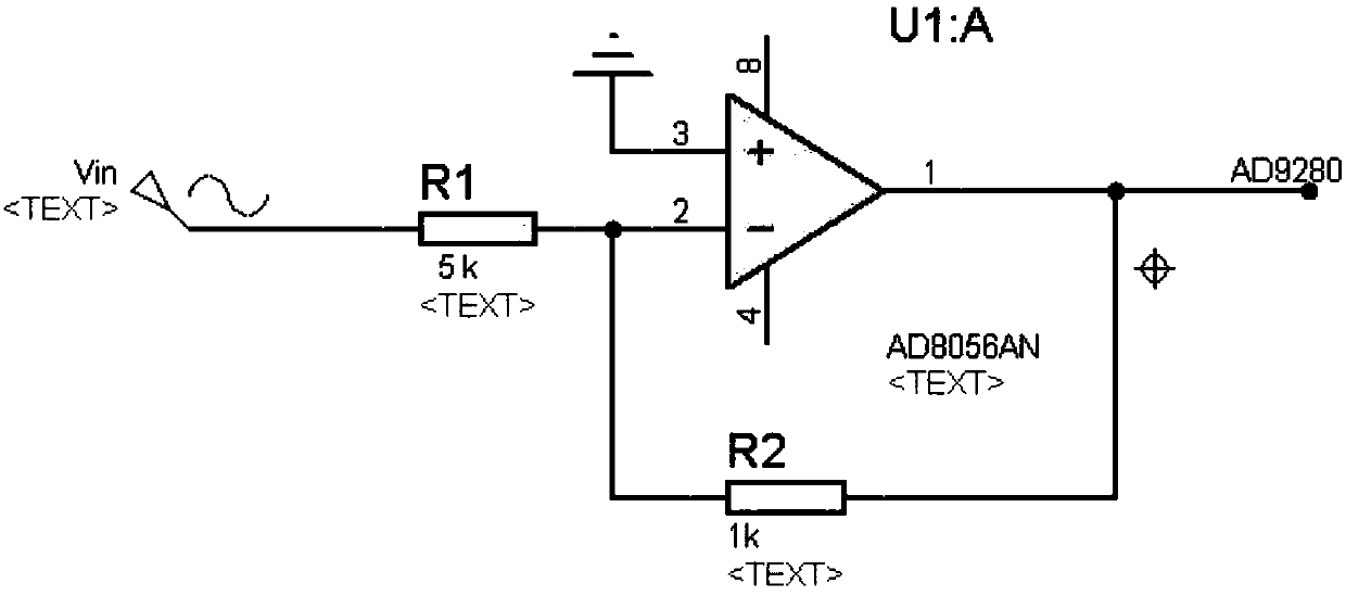
[0049] S1. Signal processing: input the analog sampling signal to the attenuation bias circuit for processing, so as to attenuate the voltage of the analog sampling signal to the input analog voltage range required by the A / D sampling circuit;

[0050]S2, A / D conversion: the analog voltage signal processed by the attenuation bias circuit is input to the A / D sampling circuit for A / D conversion, and a digital signal is output;

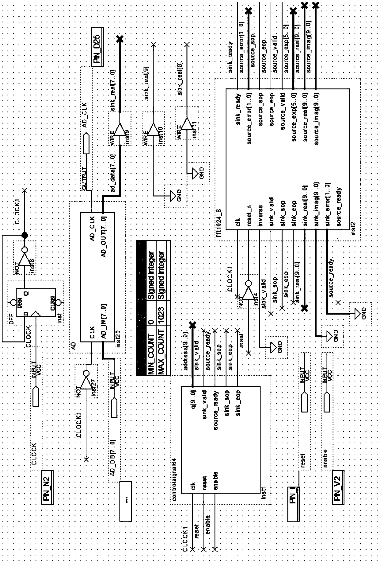
[0051] S3. FFT transformation and calculation: input the digital signal to the IP core in the FPGA, call the IP core to realize FFT transformation and calculation, and output the FFT conversion result;

[0052] S4. Spectrum analysis: Call the embedded logic analyzer, an online test tool that comes with FPGA, to perform spectrum analysis on analog sampling signals, d...

Embodiment 2

[0072] In this embodiment, subsequent IFFT and D / A processing are also carried out, so it is more intuitive to use subsequent inverse operations for verification. like Figure 5 As shown, the previous steps are basically the same as in the first embodiment, specifically: after step S3, step S31 is executed:

[0073] The FFT conversion result is input to the IP core in the FPGA, the IP core is called to perform IFFT conversion, the IFFT conversion result is input to the D / A recovery circuit, and the processed analog recovery signal is output.

[0074] Further speaking, step S31 mainly includes the following steps:

[0075] S311. The mode of the IP core is selected as IFFT transformation, and the IP core performs IFFT transformation according to the result of the FFT transformation, and outputs the first data, the last data, the exponent factor and the final result of the IFFT after the IFFT transformation;

[0076] S312. Input the final result of the IFFT to the D / A recovery ...

Embodiment 3

[0083] An FFT implementation circuit of an FPGA-based analog signal is provided, and the circuit includes:

[0084] power module;

[0085] A clock frequency division circuit is electrically connected to the power module to generate the required starting frequency;

[0086] The attenuation bias circuit is electrically connected to the power supply circuit, and is used to attenuate the voltage of the analog signal to the input analog voltage range required by the A / D sampling circuit;

[0087] The A / D sampling circuit is electrically connected with the clock frequency division circuit and the attenuation bias circuit, and is used to receive the attenuated analog voltage and convert it into a digital quantity;

[0088] The FFT control timing circuit is electrically connected with the clock frequency division circuit to generate a timing signal for controlling the FFT;

[0089] The FFT_IP core circuit is electrically connected with the clock frequency division circuit and is use...


PUM


Abstract

The present invention discloses an analog signal FFT implementation method based on an FPGA. The method comprises the steps of: S1, performing voltage attenuation of analog sampling signals to outputanalog voltage signals; S2, performing A/D conversion of the analog voltage signals to output digital signals; S3, inputting the digital signals to an IP core in the FPGA, transferring the IP core toachieve FFT transform and calculation, and outputting an FFT conversion result; S4, transferring an embedded logic analyzer in the FPGA to perform spectral analysis of the analog sampling signals, thedigital signals and the FFT conversion result; and S5, obtaining a signal frequency, a direct current component, other components and phases through calculation, and performing comparison with the signal frequency, the direct current component, the other components and the phases of the analog sampling signals. The analog signal FFT implementation method is high in transportability, can conveniently correct and process number of points of the signals, is good in real-time response, can conveniently utilize an embedded soft probe to capture and analyze the data, is fast in speed which can reach hundreds of megabytes, and is low in hardware resource occupancy rate.

Description

technical field [0001] The present invention relates to the technical field of frequency spectrum analysis of signal processing, to the frequency spectrum analysis technology of analog signals, in particular to an FPGA-based FFT implementation method of analog signals and a circuit thereof. Background technique [0002] Spectrum analysis is one of the important contents of signal processing, which refers to the method of transforming the time domain signal into the frequency domain for analysis. The purpose of spectrum analysis is to decompose the complex time history waveform into several single harmonic components through Fourier transform, so as to obtain the frequency structure of the signal and the information of each harmonic and phase. Discrete Fourier transform is the discrete spectrum of digital signals, and it is a spectrum analysis tool that can be implemented with digital circuits. [0003] Generally speaking, spectrum analysis is realized by digital methods. T...

Claims


Application Information

Patent Timeline
Patent Type & Authority Applications(China)
IPC IPC(8): G01R23/16
CPCG01R23/16
Inventor 谢智波陆智超翁海文何经杯
Owner ZHEJIANG WANLI UNIV
Why Eureka
Try Eureka