
Diode and manufacturing method thereof

A technology of diodes and silicon dioxide, which is applied in semiconductor/solid-state device manufacturing, electrical components, circuits, etc., can solve problems such as soft recovery characteristics and short reverse recovery time, achieve soft reverse recovery characteristics, and reduce reverse recovery Effect of charge and reverse recovery charge reduction

Active Publication Date: 2018-12-14
深圳市天佑照明有限公司
View PDF4 Cites 4 Cited by
  • Summary
  • Abstract
  • Description
  • Claims
  • Application Information

AI Technical Summary

Problems solved by technology

The fast recovery diodes of the traditional process can no longer meet the needs of new applications. New applications require fast recovery diodes not only to have a shorter reverse recovery time, but also to have softer recovery characteristics.

Method used

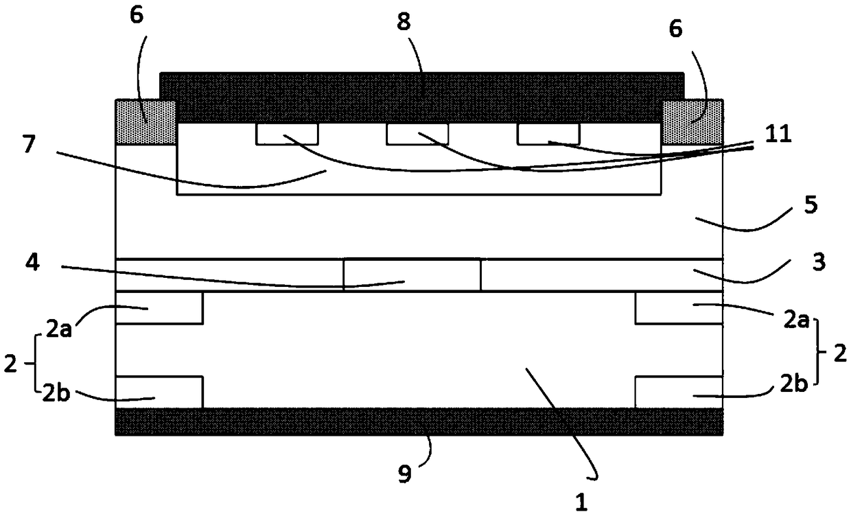
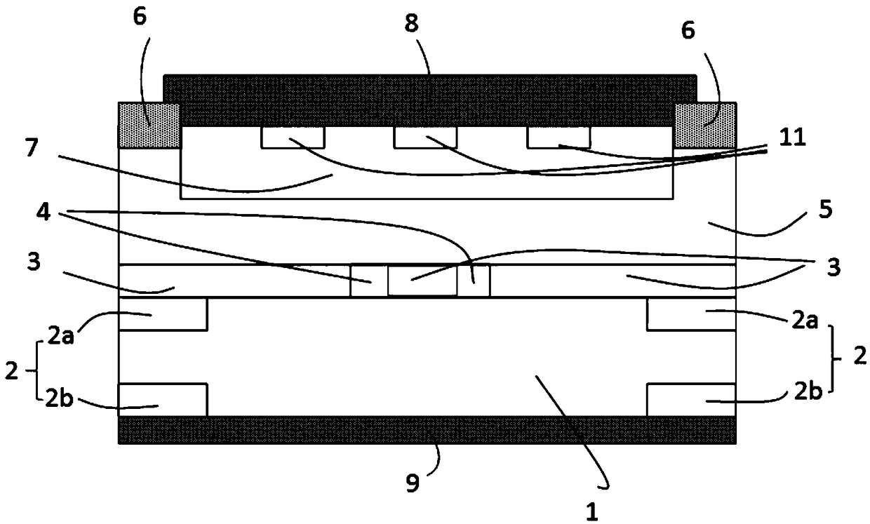
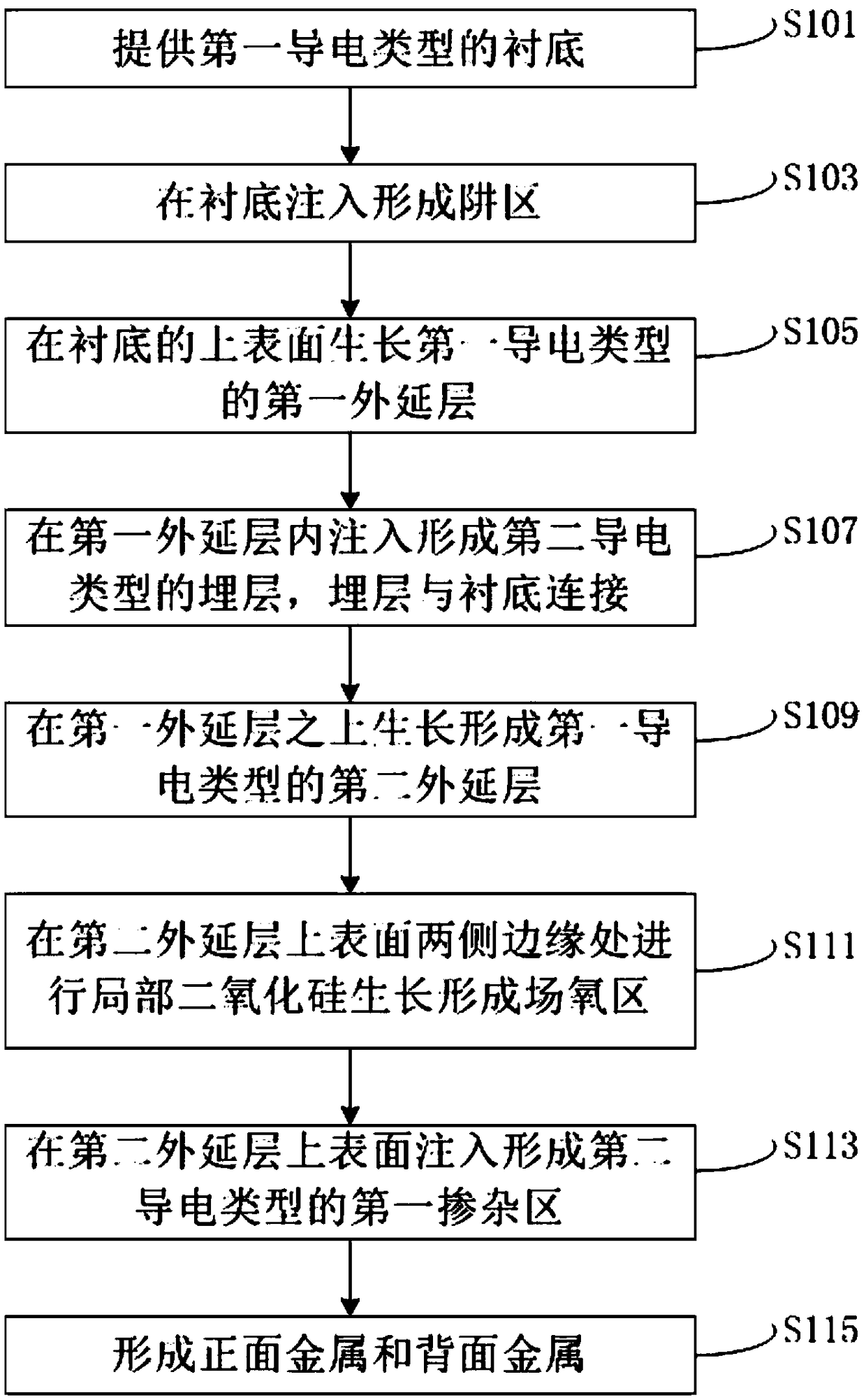

Image

  • Diode and manufacturing method thereof
  • Diode and manufacturing method thereof
  • Diode and manufacturing method thereof

Examples


Embodiment Construction

[0037] The preferred embodiments of the present invention will be described below in conjunction with the accompanying drawings. It should be understood that the preferred embodiments described here are only used to illustrate and explain the present invention, and are not intended to limit the present invention. Based on the embodiments of the present invention, all other embodiments obtained by persons of ordinary skill in the art without making creative efforts belong to the protection scope of the present invention. It should be noted that, in the case of no conflict, the embodiments of the present invention and the features in the embodiments can be combined with each other.

[0038] It should be understood that when used in this specification and the appended claims, the terms "comprising" and "comprises" indicate the presence of described features, steps, but do not exclude the presence or addition of one or more other features, steps .

[0039] In the description of t...


PUM


Abstract

A technical scheme of the invention relates to a diode and a manufacturing method thereof. The diode comprises: a substrate of a first conductivity type, well regions of a second conductivity type isformed on edges of two sides of the upper and lower surfaces of the substrate, a first epitaxial layer of a first conductivity type, a buried layer formed on the first epitaxial layer and connected tothe substrate, a second epitaxial layer of the first conductivity type, field oxygen regions formed on edges of two sides on the second epitaxial layer corresponding to the well regions, a first doped region of the second conductivity type, a front metal and a back metal formed in the second epitaxial layer. As the bury layer is provide on the first epitaxial layer, such that a parasitic avalanche diode is formed on the cathode side, As the breakdown voltage is low, the reverse recovery time can be shortened and the soft reverse recovery characteristic can be obtained. Meanwhile, the well regions of the second conductivity type are respectively injected to the upper and lower surfaces of the substrate, and the reverse recovery charge can be reduced by cooperating with the field oxygen regions, the reverse recovery time can be shortened, and the softer reverse recovery characteristic is achieved.

Description

technical field [0001] The invention relates to the technical field of semiconductors, in particular to a diode and a manufacturing method thereof. Background technique [0002] Fast recovery diode (FRD for short) is a diode with good switching characteristics and short reverse recovery time. Fast recovery diodes are widely used in switching power supplies, inverters, frequency converters, PWM pulse width modulators, motors, electrostatic induction and other fields of power electronics technology. [0003] One duty cycle of a fast recovery diode includes forward recovery and reverse recovery. The forward recovery characteristic means that the fast recovery diode can be in a stable state after a certain period of time from the forward conduction to the high transient voltage drop. The length of time reflects the forward recovery characteristic; the reverse recovery characteristic refers to the In a short period of time, the diode can recover from the forward conduction stat...

Claims


Application Information

Patent Timeline
Patent Type & Authority Applications(China)
IPC IPC(8): H01L29/06H01L21/329H01L29/861
CPCH01L29/0661H01L29/6609H01L29/861
Inventor 阳林涛王永贵
Owner 深圳市天佑照明有限公司
Learn More