Fabrication method of micro-nano structure and system used in the fabrication method

A production method and technology of micro-nano structure, applied in the direction of photo-plate-making process of pattern surface, micro-lithography exposure equipment, photo-plate-making process exposure device, etc., can solve the problems of lower resolution of nano-processing and lower precision of micro-nano structure

Inactive Publication Date: 2018-12-18
SHENZHEN INST OF ADVANCED TECH
View PDF5 Cites 2 Cited by
  • Summary
  • Abstract
  • Description
  • Claims
  • Application Information

AI Technical Summary

Problems solved by technology

However, in the process of heating the mask material by laser, the thermal diffusion effect will expand the area where the thermal exposure causes the phase chan

Method used


Image

  • Fabrication method of micro-nano structure and system used in the fabrication method
  • Fabrication method of micro-nano structure and system used in the fabrication method
  • Fabrication method of micro-nano structure and system used in the fabrication method

Examples


Embodiment 1

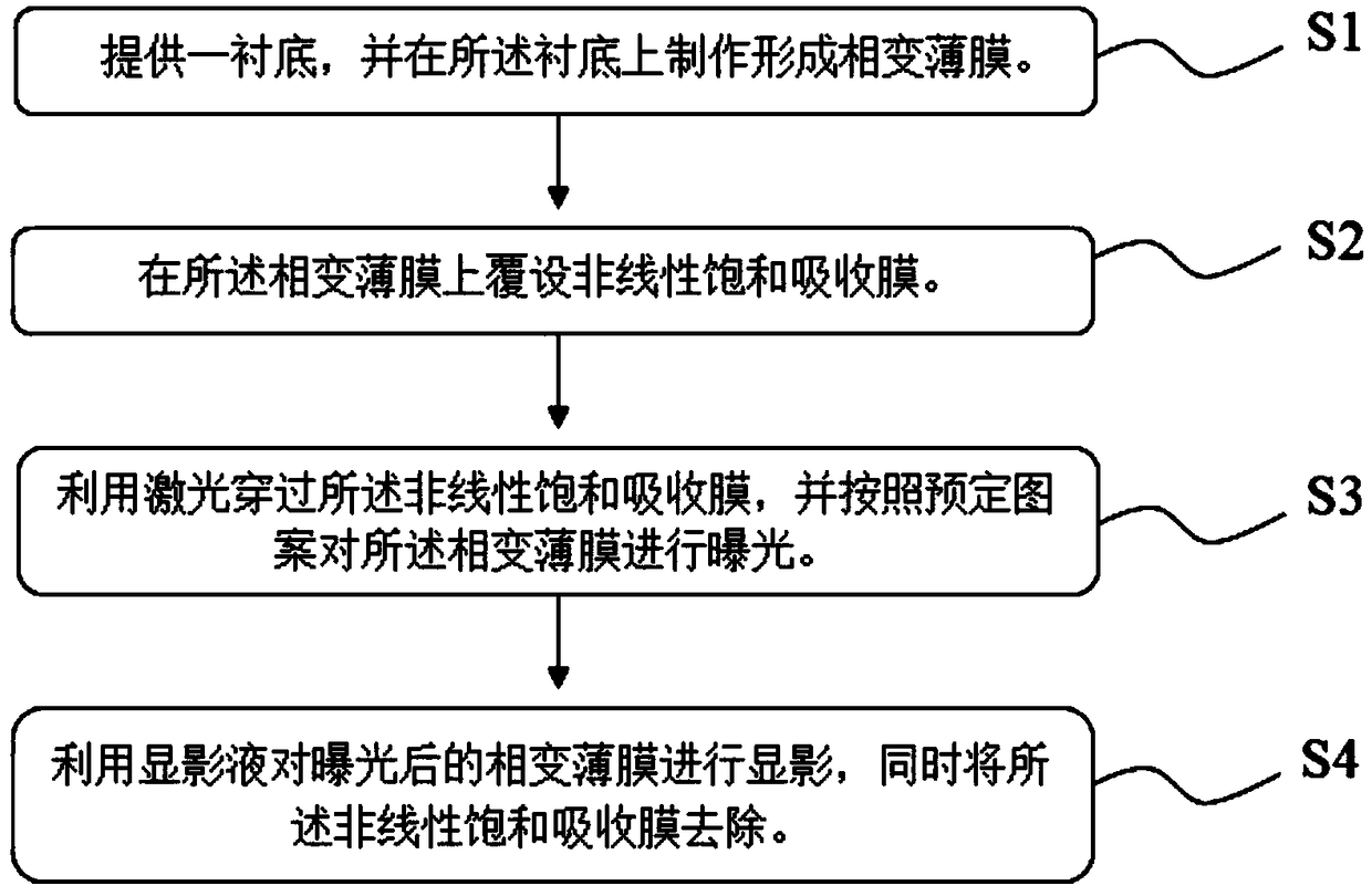
[0029] refer to figure 1 , the present embodiment provides a method for fabricating a micro-nano structure, comprising the steps of:

[0030] S1. Provide a substrate, and fabricate and form a phase change film on the substrate;

[0031] S2. Covering the phase change film with a nonlinear saturable absorption film;

[0032] S3, using a laser to pass through the nonlinear saturable absorption film, and exposing the phase change film according to a predetermined pattern;

[0033] S4. Using a developing solution to develop the exposed phase change film, and remove the nonlinear saturable absorption film at the same time.

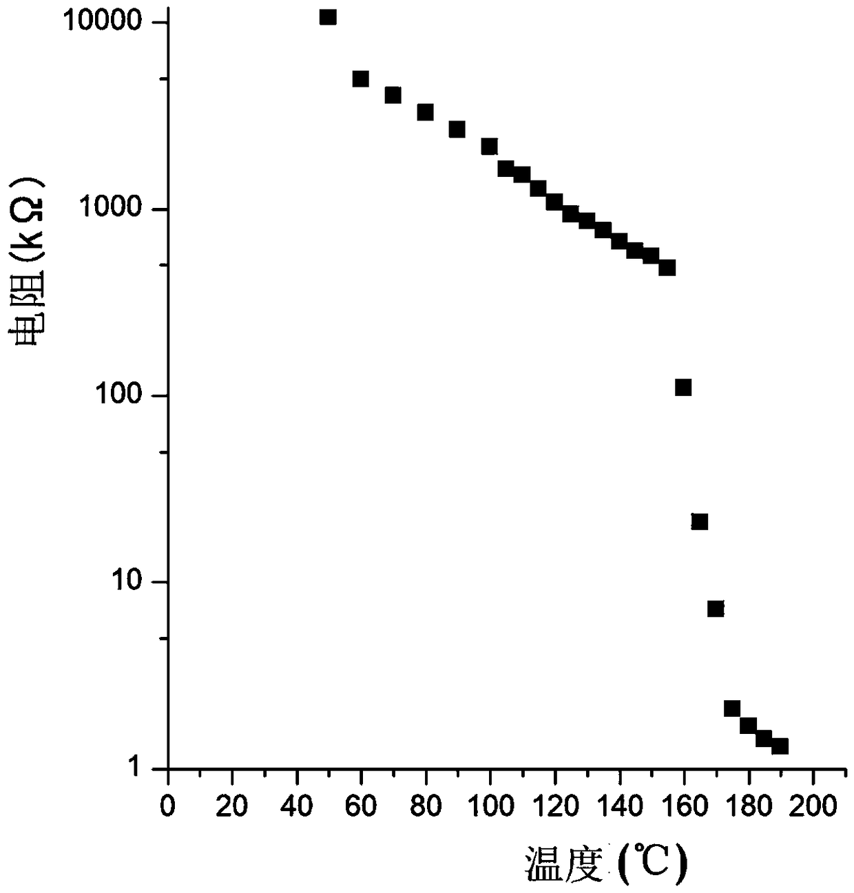
[0034] The fabrication method of the micro-nano structure provided by the present invention exposes the phase-change thin film by passing the laser through the nonlinear saturable absorption film, and utilizes the nonlinear saturable absorption characteristics of the nonlinear saturable absorption film, and the nonlinear saturable absorption The absorption of...

Embodiment 2

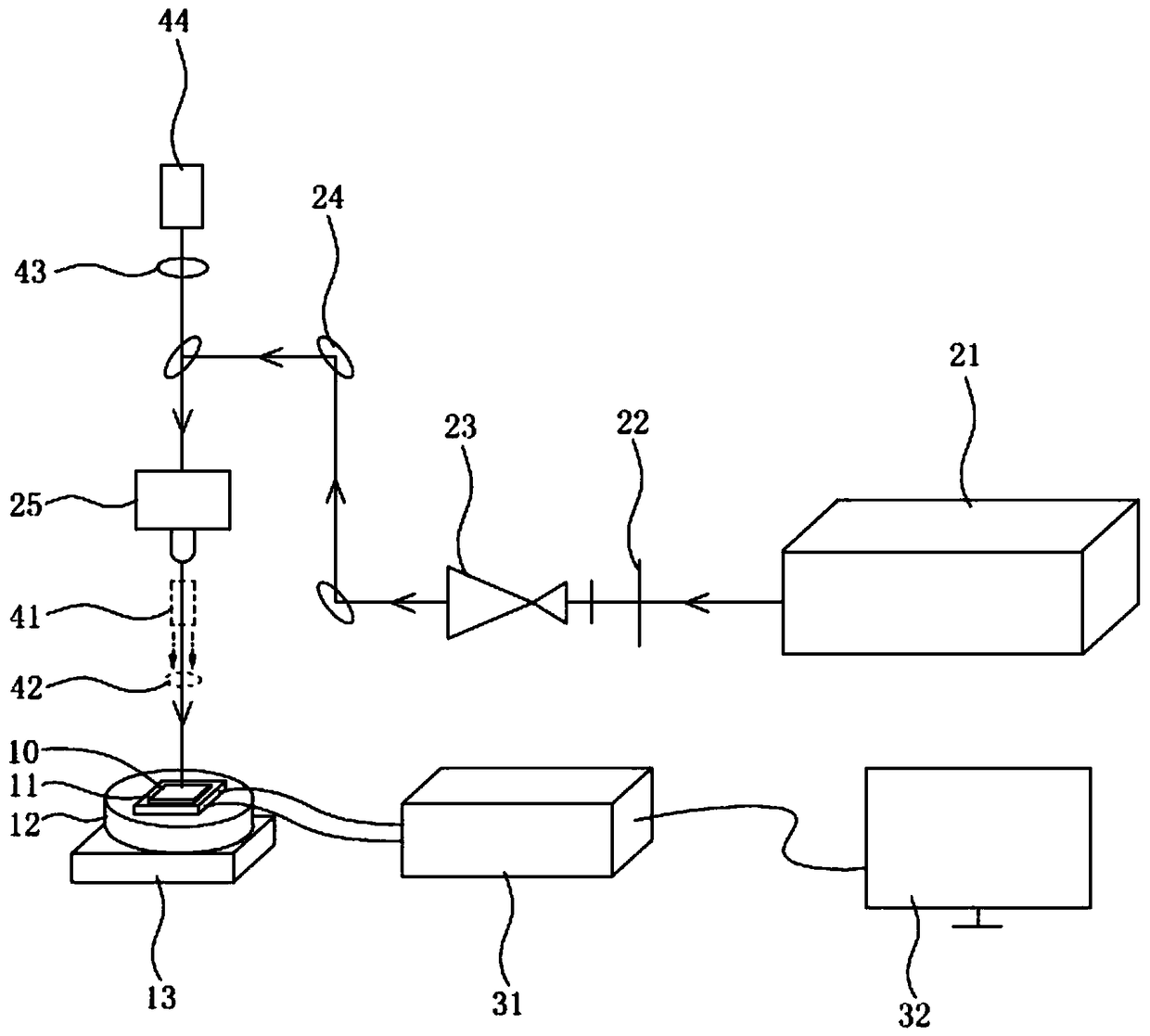
[0045] Such as figure 2 As shown, this embodiment also provides a system used in the above-mentioned method for fabricating the micro-nano structure, which is mainly applied in the above-mentioned step S3. The system includes a piezoelectric stage, a laser component, a control component and an imaging component. Wherein, the piezoelectric stage is used to carry an object, and the signal generated by pressing the object on the piezoelectric stage is transmitted to the control component; the laser component is used to emit laser light to irradiate the object; The control component is used to determine the position of the object on the piezoelectric stage according to the signal, and is used to move the object according to a predetermined pattern; the imaging component is used to image the object to Monitor the object.

[0046] Specifically, the piezoelectric stage includes a manual lifting platform 13, a manual translation platform 12, and a piezoelectric seat 11 stacked in s...


PUM

PropertyMeasurementUnit
Thicknessaaaaaaaaaa
Thicknessaaaaaaaaaa
Thicknessaaaaaaaaaa

Abstract

The invention provides a fabrication method of a micro-nano structure and a system used in the fabrication method. The fabrication method comprises the following steps: a substrate is provided and a phase change film is formed on the substrate; a non-linear saturated absorption film is coated on the phase change film; laser is used to pas through that nonlinear saturation absorption film, and thephase change film is exposed according to a predetermined pattern; and the exposed phase change film is developed using a developer, and the nonlinear saturation absorption film is removed at the sametime. According to the method, the nonlinear saturate absorption film is arranged to cover the phase change film, laser passes through the nonlinear saturated absorption film and the phase change film is exposed to fabricate the micro-nano structure, thus a laser beam is more concentrated, light spots are shrinked and the precision of the micro-nano structure is improved; and on the other hand, femtosecond laser is selected as a laser source, the thermal effect of laser is prevented from affecting the unexposed area, and thus the precision of the micro-nano structure is further improved.

Description

technical field [0001] The invention relates to the technical field of manufacturing micro-nano structures, in particular to a method for manufacturing micro-nano structures and a system used in the manufacturing method. Background technique [0002] In the prior art, the laser direct writing technology is a commonly used micro-nano structure manufacturing process, which can use the intensity-adjustable laser to expose the resist material with variable doses, so that after the resist material is developed, the A micro-nano structure with a specified pattern is formed on the surface. However, the current laser direct writing technology is limited by the optical diffraction limit of the spot size of the direct writing laser beam, which limits the precision of the formed micro-nano structure. Generally, this technology can only produce micro-nano structures with an accuracy of more than 1 micron. It limits its application in the field of nanoscale structure fabrication and dev...

Claims


Application Information

Patent Timeline
IPC IPC(8): G03F7/00G03F7/20
CPCG03F7/0035G03F7/70025
Inventor 陶华露李文杰童君程冠铭冯叶隋帆李伟民钟国华杨春雷
Owner SHENZHEN INST OF ADVANCED TECH
Why Eureka
Try Eureka