N-Ti-Sb-Te-based synaptic biomimetic device used in artificial neural network

A synaptic device, synaptic technology, applied in biological neural network models, electrical components, physical implementation, etc., can solve the problems of poor linear change, excessive high and low resistance differences, low bit resolution, etc., and achieve excellent electrical properties. Effect

Active Publication Date: 2018-12-18
HANGZHOU DIANZI UNIV
View PDF10 Cites 0 Cited by
  • Summary
  • Abstract
  • Description
  • Claims
  • Application Information

AI Technical Summary

Problems solved by technology

However, the factors that limit the performance of artificial neural networks using non-volatile memory are the poor linear change of the resistance of the synaptic device to the number of pulses, the low bit resolution, and the large or small difference between high and low resistance.

Method used


Image

  • N-Ti-Sb-Te-based synaptic biomimetic device used in artificial neural network
  • N-Ti-Sb-Te-based synaptic biomimetic device used in artificial neural network
  • N-Ti-Sb-Te-based synaptic biomimetic device used in artificial neural network

Examples


Embodiment 1

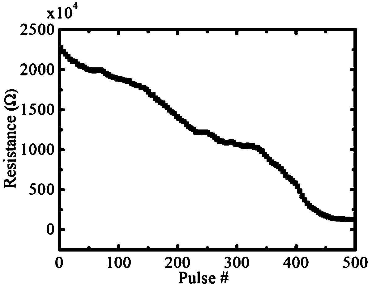
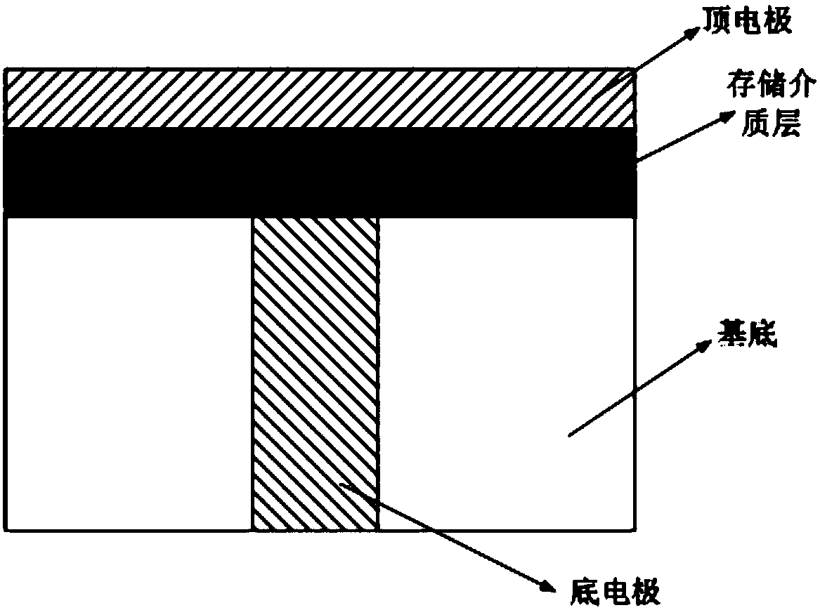
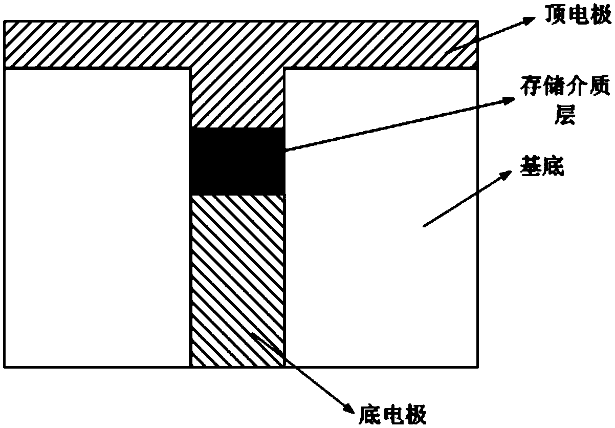
[0045] Example 1: An electrode in a medium with a diameter of 190 nanometers was prepared using a standard 0.13 micron CMOS process. The storage medium layer is deposited by physical vapor deposition with a thickness of 120 nanometers, and the N layer above the electrode is prepared through glue coating, photolithography, etching and other processes. 5 (TiSb 5 Te 7.5 ) 95 material pattern such that each bottom electrode above the N 5 (TiSb 5 Te 7.5 ) 95 The materials are electrically insulated from each other. The top electrode titanium nitride TiN is deposited by physical vapor deposition method, with a thickness of 20 nanometers, and the N 5 (TiSb 5 Te 7.5 ) 95 above the TiN electrode material graph so that each N 5 (TiSb 5 Te 7.5 ) 95 The upper top electrode materials are electrically insulated from each other. get based on N 5 (TiSb 5 Te 7.5 ) 95 The T-shaped synaptic bionic unit of the material; and the performance parameters of this product are that th...

Embodiment 2

[0046] Example 2: An electrode in a medium with a diameter of 190 nanometers was prepared using a standard 0.13 micron CMOS process. The storage medium layer is deposited by chemical vapor deposition with a thickness of 200 nanometers, and the N layer above the electrode is prepared through glue coating, photolithography, etching and other processes. 0.1 (TiSb 40 Te 10 ) 99.9 material pattern such that each bottom electrode above the N 0.1 (TiSb 40 Te 10 ) 99.9 The materials are electrically insulated from each other. The top electrode titanium nitride TiN was deposited by physical vapor deposition with a thickness of 200 nm, and N was prepared by coating, photolithography, and etching. 0.1 (TiSb 40 Te 10 ) 99.9 above the TiN electrode material graph so that each N 0.1 (TiSb 40 Te 10 ) 99.9 The upper top electrode materials are electrically insulated from each other. get based on N 0.1 (TiSb 40 Te 10 ) 99.9 The T-shaped synaptic bionic unit of the material; ...

Embodiment 3

[0047] Example 3: An electrode in a medium is prepared by using a standard CMOS process, with a diameter of 10 nanometers. The storage medium layer is deposited by chemical vapor deposition with a thickness of 50 nanometers, and the N layer above the electrode is prepared through glue coating, photolithography, etching and other processes. 3 (TiSb 10 Te 10 ) 97 material pattern such that each bottom electrode above the N 3 (TiSb 10 Te 10 ) 97 The materials are electrically insulated from each other. The top electrode titanium nitride TiN is deposited by physical vapor deposition method, with a thickness of 20 nanometers, and the N 3 (TiSb 10 Te 10 ) 97 above the TiN electrode material graph so that each N 3 (TiSb 10 Te 10 ) 97 The upper top electrode materials are electrically insulated from each other. get based on N 3 (TiSb 10 Te 10 ) 97 The T-shaped synaptic bionic unit of the material; and the performance parameters of the product are that the difference...


PUM


Abstract

The invention discloses an N-Ti-Sb-Te-based synaptic biomimetic device used in an artificial neural network. The storage medium used for preparing the synaptic biomimetic device is Nx(TiSbyTez)100-X,where 0.1 <= x <= 5, 0.25 <= y/z <= 4, 12 <= y + z <= 50. This material can realize the repeated conversion of high and low resistance value of polymorphism under the operation of electric signal, andkeep the resistance value unchanged without the operation signal. Where 500 picoseconds <= electrical signal pulse width <= 500 nanoseconds. The synaptic biomimetic device based on N-Ti-Sb- Te seriesphase change material has excellent electrical properties as a synaptic biomimetic device under the operation of electrical signals, in which the interstate resistance value can provide nearly 8 bitsresolution and the difference of switching resistance is 1000 times. The linear response of the resistance to the number of pulses is realized under the same pulse operation, and the synaptic biomimetic devices have excellent electrical properties.

Description

technical field [0001] The invention relates to the field of semiconductor manufacturing materials and semiconductor devices, in particular to a storage medium material and a device for manufacturing synaptic bionic devices in artificial neural networks. Background technique [0002] Artificial Neural Network (ANN) is a research hotspot in the field of artificial intelligence since the 1980s. It abstracts the human brain neuron network from the perspective of information processing, establishes a simple model, and forms different networks according to different connection methods. In engineering and academia, it is often referred to directly as a neural network or a neural network. A neural network is an operational model consisting of a large number of nodes (or neurons) connected to each other. Each node represents a specific output function called an activation function. Each connection between two nodes represents a weighted value for the signal passing through the co...

Claims


Application Information

Patent Timeline
Patent Type & Authority Applications(China)
IPC IPC(8): H01L45/00G06N3/063
CPCG06N3/063H10N70/8828
Inventor 任堃赵哲昊季振国
Owner HANGZHOU DIANZI UNIV
Why Eureka
Try Eureka