Neural synapse bionic device with mushroom-shaped structure

A nerve synapse, mushroom-type technology, applied in electrical components and other directions, can solve the problems of loss of phase transition performance, slow phase transition speed, and inability to be used in phase change memory and synaptic devices.

Pending Publication Date: 2021-07-30
JIANGSU UNIV OF TECH
View PDF3 Cites 0 Cited by
  • Summary
  • Abstract
  • Description
  • Claims
  • Application Information

AI Technical Summary

Problems solved by technology

[0004] Chinese patent CN106206943B discloses a nitrogen-doped modified phase-change thin film material and its preparation method. Doping foreign N atoms in the Zn-Sb material can increase the phase transition temperature of the material, but too much N atom

Method used


Image

  • Neural synapse bionic device with mushroom-shaped structure
  • Neural synapse bionic device with mushroom-shaped structure
  • Neural synapse bionic device with mushroom-shaped structure

Examples


Embodiment 1

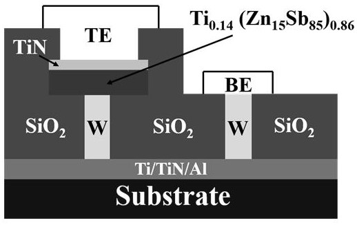
[0022] This embodiment provides a Ti-based 0.14 (Zn 15 Sb 85 ) 0.86 The mushroom-shaped structure neurosynaptic biomimetic device of the storage medium, the structure is as follows figure 1 As shown, the thickness of the storage medium is 50 nm, and the specific preparation steps are:

[0023] 1. Clean the 190 nm W column bottom electrode substrate to remove dust particles, organic and inorganic impurities on the surface of the substrate:

[0024] (a) Place the substrate in an acetone solution, clean it with strong ultrasound for 10 minutes, and rinse it with deionized water for 5 minutes;

[0025] (b) Place the substrate in an ethanol solution, clean it with strong ultrasound for 10 minutes, and then rinse it with deionized water for 5 minutes;

[0026] (c) Take out the substrate and use high-purity N 2 Blow dry the surface and the back, and place it in a 60°C constant temperature drying oven to be dried;

[0027] 2. Preparation of Nanocomposite Ti by Magnetron Sputte...


PUM

PropertyMeasurementUnit
Diameteraaaaaaaaaa
Thicknessaaaaaaaaaa
Thicknessaaaaaaaaaa

Abstract

The invention discloses a mushroom-shaped structure nerve synapse bionic device, which is of a mushroom-shaped structure prepared by adopting a 0.13-micron CMOS process, and comprises a substrate prepared from a Si (100) substrate, an Al material bottom electrode, a SiO2 intermediate dielectric layer, a W heating electrode formed on the intermediate dielectric layer, a Ti-Zn-Sb storage medium layer, a TiN adhesion layer and an Al material top electrode from bottom to top in sequence. The Ti<x>(Zn<y>Sb<100-y>)<1-x> phase change material is used as a storage medium in the neural synapse bionic device, conversion among multi-state resistance values can be realized under the action of 5-500 ns electric signal pulse width, an intermediate-state resistance value can provide about 8-bit resolution, and the switch resistance difference is about 2 orders of magnitude. Under the same pulse operation, the linear response of the resistor to the number of pulses can be realized, and the electrical property requirement of the synaptic bionic device is met.

Description

technical field [0001] The invention belongs to the technical field of semiconductor devices, and in particular relates to a bionic device of a mushroom-shaped structure nerve synapse. Background technique [0002] Synapse is the smallest unit of learning and memory in the human brain. It receives external stimulation signals to make neurons excitatory and inhibitory, thereby inputting and outputting signals. The biomimetic simulation of synapse learning function is considered to be an important means to realize artificial neural network. Synaptic devices are mainly used to connect neurons, and their poor performance directly affects the efficiency and accuracy of artificial neural network processing. Lu et al. discovered a nano-silicon-based memristor, which can simulate the basic properties of synapses, and has efficient computing methods and densities (Nano Letters, 2010, 10(4): 1297-1301). Wang et al proposed a biomimetic device based on amorphous InGaZnO synapses, whi...

Claims


Application Information

Patent Timeline
IPC IPC(8): H01L45/00
CPCH10N70/231H10N70/881
Inventor 吴卫华戚佳怡汤瑶朱小芹薛建忠
Owner JIANGSU UNIV OF TECH
Why Eureka
Try Eureka