A solar cell crystal silicon insertion device

A technology of solar cells and crystalline silicon, applied in circuits, photovoltaic power generation, electrical components, etc., can solve problems such as poor quality, damage to single crystal silicon wafers, and low efficiency, and achieve the effects of improving stability, improving protection, and improving quality

Pending Publication Date: 2018-12-21
天长市百盛半导体科技有限公司
View PDF0 Cites 2 Cited by
  • Summary
  • Abstract
  • Description
  • Claims
  • Application Information

AI Technical Summary

Problems solved by technology

In the production process of monocrystalline silicon wafers, it is necessary to use a special monocrystalline silicon wafer storage device to insert the monocrystalline silicon wafers into the corresponding limit slots, and then transport and store them. The existing wafer insertion equipment has low efficiency. The quality is poor, and it is easy to cause damage to the monocrystalline silicon wafer, so it is urgent to develop a high-efficiency and high-quality solar cell crystalline silicon insertion device to solve the problems in the prior art

Method used


Image

  • A solar cell crystal silicon insertion device
  • A solar cell crystal silicon insertion device
  • A solar cell crystal silicon insertion device

Examples


Embodiment 1

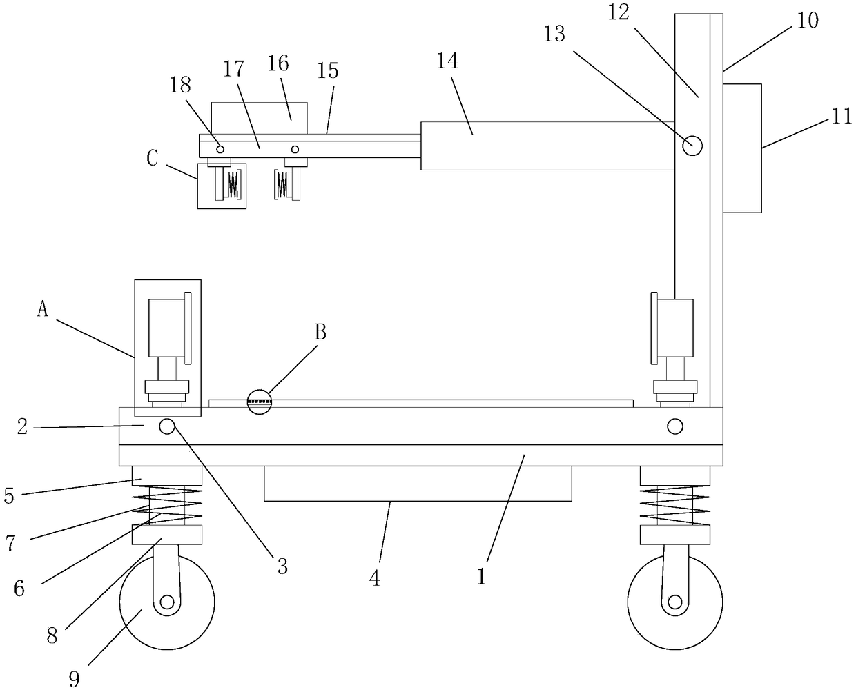
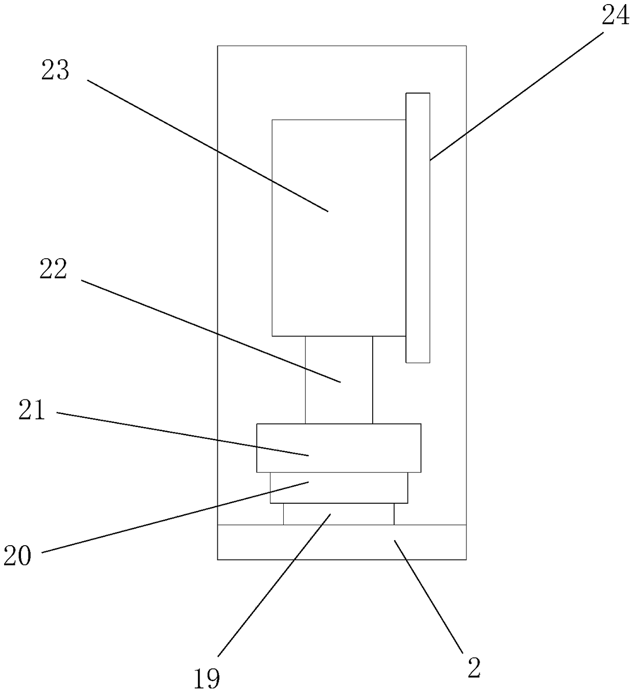
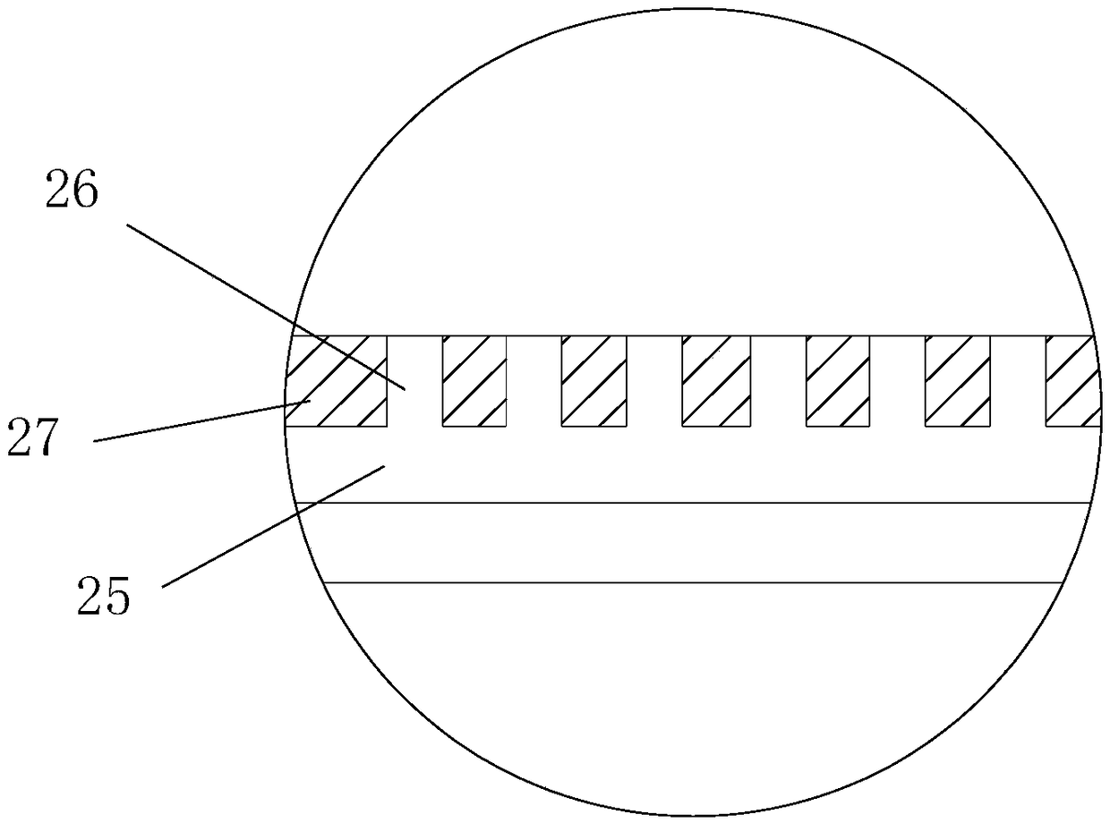
[0031] Such as Figure 1-6As shown, the present invention provides a solar cell crystalline silicon insert device, including a base 1 and a first limit seat 27 arranged on the upper end of the base 1, the base 1 is provided with a first chute 2, and the first chute 2 is symmetrical to the other. The center line is provided with a pair of first pulleys 3, the first slide plate 19 is installed on the first pulley 3, the end of the first slide plate 19 away from the first pulley 3 is equipped with a first mounting plate 20, the first mounting plate 20 is far away from the first A third piston 21 is installed on one end of the slide plate 19, a third piston shaft 22 is installed on the end of the third piston 21 away from the first mounting plate 20, and a first elastic plate is installed on the end of the third piston shaft 22 away from the third piston 21. Seat 23, a first elastic plate 24 is installed on one side of the first elastic plate mounting seat 23, the base 1 upper end...


PUM


Abstract

The invention discloses a solar cell crystal silicon insertion device, the first mounting plate slides on the first sliding groove through the first pulley, A third piston and a third piston shaft aremounted on the first mounting plate, A first elastic plate is mounted on the third piston shaft through a first elastic plate mounting seat, the first piston slides on the second sliding groove through the second pulley, A first piston shaft is mounted on the first piston, A third sliding groove is arranged in the first piston shaft, The second slide plate slides on the third slide groove througha third pulley, the second slide plate is mounted with a second mounting plate, a fourth piston is mounted on one side of the second mounting plate, a fourth piston and a fourth piston shaft are mounted on the fourth piston, and a second elastic plate is mounted on the fourth piston shaft through a second elastic plate mounting seat. The invention can effectively improve the chip insertion efficiency and quality of the single crystal silicon wafer.

Description

technical field [0001] The invention relates to the technical field of monocrystalline silicon wafer processing equipment, in particular to a solar cell crystalline silicon inserting device. Background technique [0002] Monocrystalline silicon is a relatively active non-metallic element, an important part of crystalline materials, and is at the forefront of the development of new materials. Its main uses are as semiconductor materials and the use of solar photovoltaic power generation, heating and so on. Because solar energy has many advantages such as cleanliness, environmental protection, and convenience, solar energy utilization technology has made great progress in research and development, commercial production, and market development in the past 30 years, and has become one of the emerging industries with rapid and stable development in the world. Monocrystalline silicon can be used in the production and deep processing of diode level, rectifier level, circuit level ...

Claims


Application Information

Patent Timeline
IPC IPC(8): H01L21/673H01L31/18
CPCH01L31/1804H01L21/673Y02E10/547Y02P70/50
Inventor 刘宏王春定龚志国姚学森刘柏林
Owner 天长市百盛半导体科技有限公司
Why Eureka
Try Eureka