Micro-LED mass transfer method and Micro-LED substrate

A transfer method and transfer plate technology, which are applied in the manufacturing of semiconductor devices, electrical components, semiconductor/solid-state devices, etc., to achieve the effect of simple and effective assembly method, improving production yield, and avoiding collisions

Inactive Publication Date: 2018-12-21
BOE TECH GRP CO LTD +1
View PDF4 Cites 41 Cited by
  • Summary
  • Abstract
  • Description
  • Claims
  • Application Information

AI Technical Summary

Problems solved by technology

However, the bottleneck restricting the development of Micro-LED display technology mainly includes mass transfer technology

Method used


Image

  • Micro-LED mass transfer method and Micro-LED substrate
  • Micro-LED mass transfer method and Micro-LED substrate
  • Micro-LED mass transfer method and Micro-LED substrate

Examples


Embodiment Construction

[0060] In order to make the purpose, technical solutions and advantages of the embodiments of the present invention more clear, the following will clearly and completely describe the technical solutions of the embodiments of the present invention in conjunction with the drawings of the embodiments of the present invention. Apparently, the described embodiments are some, not all, embodiments of the present invention. All other embodiments obtained by those skilled in the art based on the described embodiments of the present invention belong to the protection scope of the present invention.

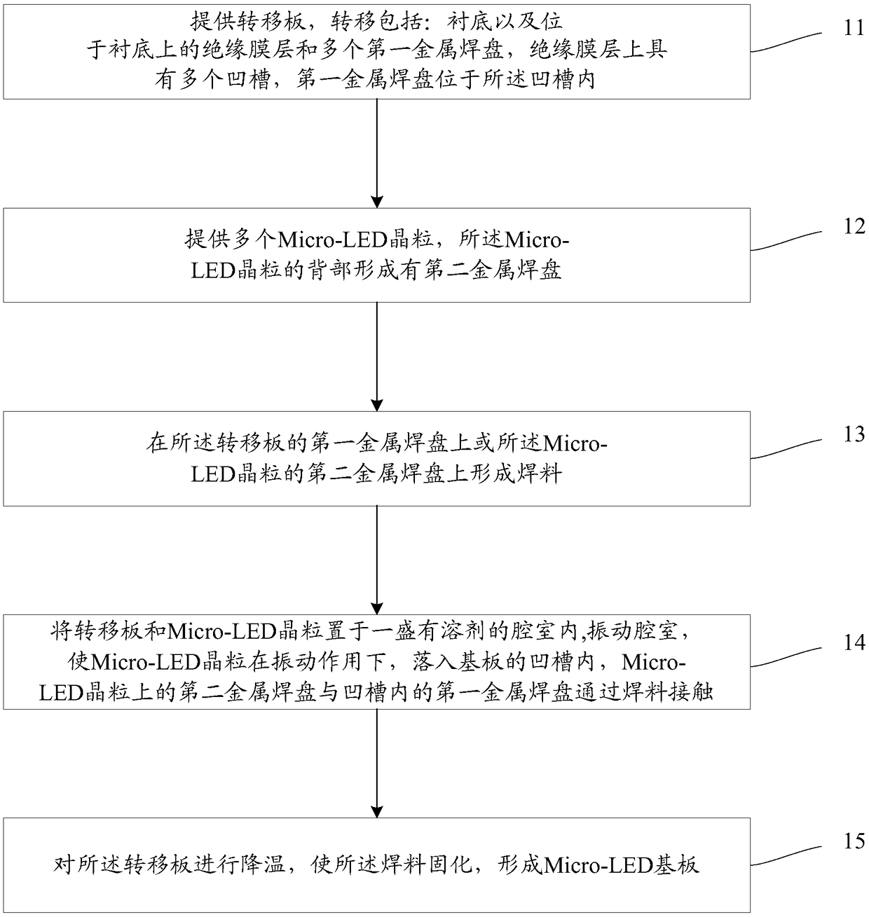
[0061] Please refer to him 1, figure 1 It is a schematic flow chart of a Micro-LED mass transfer method according to an embodiment of the present invention. The method includes:

[0062] Step 11: Provide a transfer board, the transfer board includes: a substrate, an insulating film layer on the substrate and a plurality of first metal pads, and the insulating film layer has a plurality of ...


PUM


Abstract

The invention provides a Micro-LED massive transfer method and a Micro-LED substrate, the method comprises: providing a transfer plate, wherein the transfer plate comprise a substrate, an insulating film layer on the substrate and a plurality of first metal pads, wherein the insulating film layer has a plurality of grooves, and the first metal pads are positioned in the grooves; providing multipleMicro-LED dies,wherein the back of the Micro-LED die has a second metal pad; forming solder on the first metal pad or on the second metal pad; placing the transfer plate and Micro-LED dies in a chamber containing solvent, and vibrating the chamber so that the Micro-LED dies fall into the groove of the transfer plate,the second metal pad on the Micro-LED dies is in contact with the first metal padin the groove through the solder, and the temperature in the chamber is higher than the melting point of the solder; and solidifying the solder. The Micro-LED massive transfer method has high yield and low cost.

Description

technical field [0001] The present invention relates to the field of Micro-LED technology, in particular to a Micro-LED mass transfer method and a Micro-LED substrate. Background technique [0002] Micro-LED (miniature light-emitting diode) is a new generation of display technology, which has higher brightness and better luminous efficiency than the existing OLED (organic light-emitting diode) technology, but lower power consumption. Micro-LED technology, the LED structure design is thinned, miniaturized, and arrayed, and its size is only about 1-10 μm. The biggest advantage of Micro-LED comes from the micron-level pitch, each pixel (pixel) can be addressed and controlled and single-point driven to emit light, long life, and wide application range. However, the bottleneck restricting the development of Micro-LED display technology mainly includes mass transfer technology. Mass transfer technology, that is, how to transfer a large number of micro-scale Micro-LED grains to l...

Claims


Application Information

Patent Timeline
Patent Type & Authority Applications(China)
IPC IPC(8): H01L33/00H01L25/075
CPCH01L25/0753H01L33/0093H01L33/62H01L2224/83801H01L2224/29101H01L2924/12041H01L2224/83191H01L2224/83192H01L2224/83815H01L24/95H01L24/83H01L24/29H01L2224/95085H01L24/75H01L2224/75101H01L2224/755H01L2224/7525H01L24/05H01L2224/04026H01L2224/95122H01L2224/95133H01L2224/27422H01L24/27H01L2924/00014H01L2924/014H01L21/67739H01L27/156H01L33/005
Inventor 邹振游李梁梁霍亚洲孟凡清伍蓉席文星孔凯斌
Owner BOE TECH GRP CO LTD
Why Eureka
Try Eureka