
A driver based on a gallium nitride power device and a printed circuit layout

A power device, gallium nitride technology, applied in the output power conversion device, the conversion of AC power input to DC power output, electrical components and other directions, can solve the problem of large conduction voltage drop, reduce voltage spikes, suppress gate Pole drive oscillation, cost reduction effect

Pending Publication Date: 2018-12-21
NORTHWESTERN POLYTECHNICAL UNIV
View PDF2 Cites 12 Cited by
  • Summary
  • Abstract
  • Description
  • Claims
  • Application Information

AI Technical Summary

Problems solved by technology

[0008] The publication number is CN102611288A, the application date is March 19, 2012, and the publication date is July 25, 2012. The Chinese patent proposes a three-level drive method for GaN power transistors. This patent is aimed at GaN power transistors. The problem of the large conduction voltage drop of the transistor under the reverse conduction mechanism, reducing the reverse conduction loss, can improve the working efficiency of the converter to a certain extent, but there are similar problems with regard to the driving method and the publication number CN105896992A, which will not be discussed here repeat

Method used


Image

  • A driver based on a gallium nitride power device and a printed circuit layout
  • A driver based on a gallium nitride power device and a printed circuit layout
  • A driver based on a gallium nitride power device and a printed circuit layout

Examples


specific Embodiment

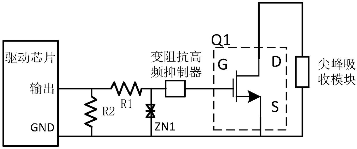
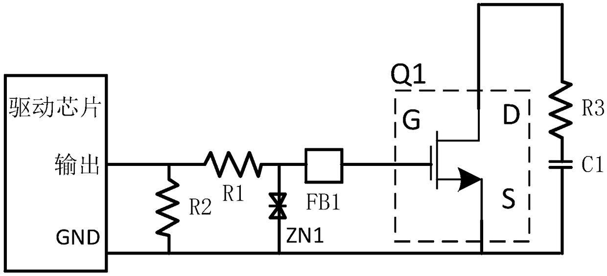
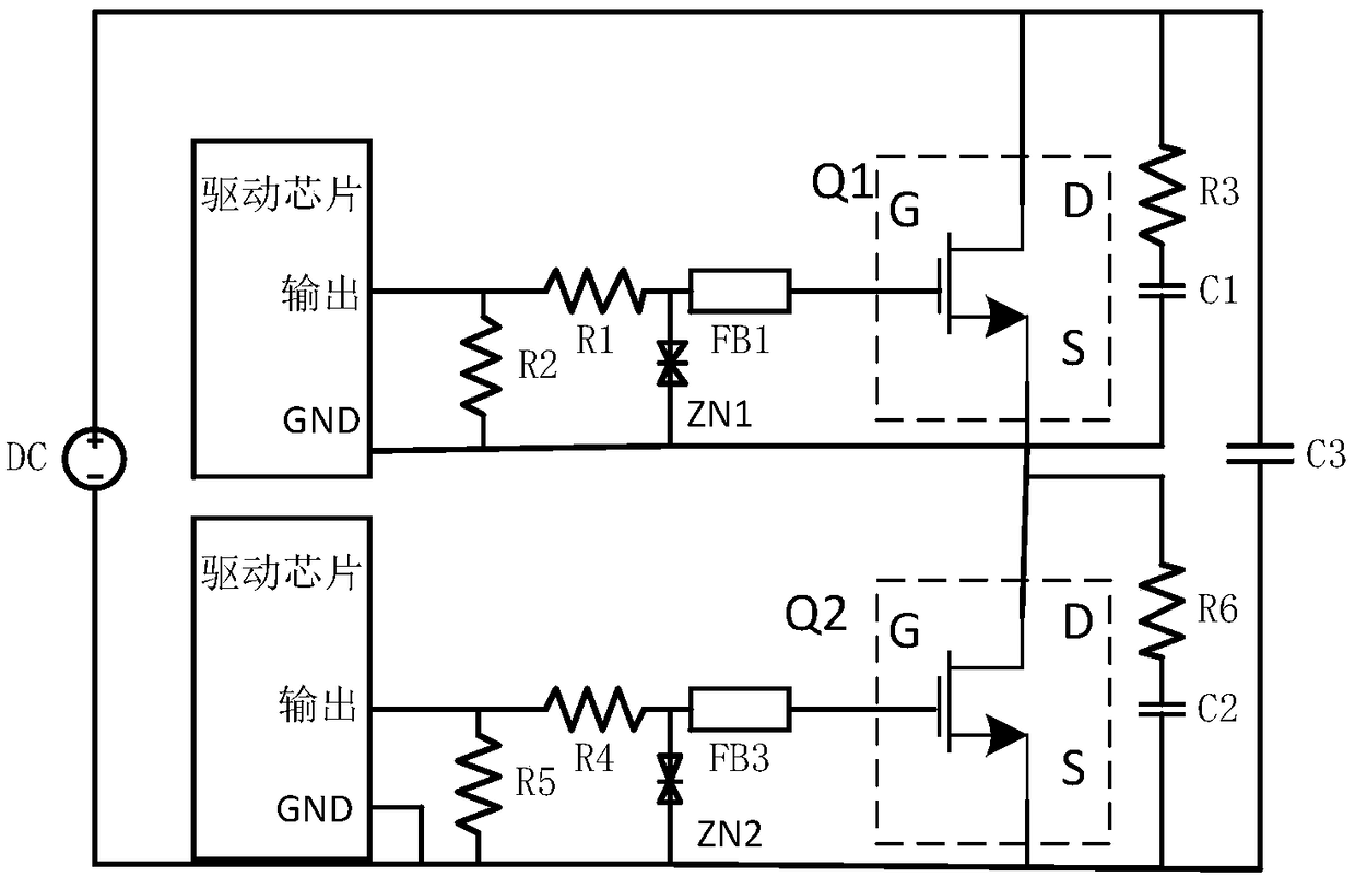
[0040] figure 1 It is a circuit diagram of the present invention, the circuit includes a driver chip, a first resistor R1, a second resistor R2, a variable impedance high-frequency suppressor, a gallium nitride power transistor, a first Zener diode ZN1 and a peak absorption module; the driver chip The output end is connected to one end of the first resistor R1 and the second resistor R2, and the other end of the first resistor R1 is connected to the variable impedance high frequency suppressor and the first stabilizer One end of the voltage diode, the other end of the variable impedance high-frequency suppressor is connected to the gate of the GaN power transistor; then the other end of the second resistor R2 is connected to the first regulator The other end of the diode ZN1 is commonly connected to the source of the GaN power transistor; one end of the peak absorption module is connected to the drain of the GaN transistor, and the other end is connected to the source of the G...


PUM


Abstract

The invention relates to a driver based on a gallium nitride power device and a printed circuit layout. A resistor R2, a resistor R1, a variable impedance high-frequency suppressor, a voltage regulating diode and a spike absorption module are between the gallium nitride power transistor and a driving chip. The resistor R2 is connected in parallel to an output terminal of the resistor R2, a resistor R1 and a variable impedance high-frequency suppressor are connected in series are connected with a gate of a GaN power transistor de, and a voltage stabilizing diode is connected in parallel with the resistor R1 and the variable impedance high-frequency suppressor and is connected with an output terminal GND of the driving chip. The spike absorption module is connected in parallel to the drain and source of the output of the gallium nitride power transistor. The invention can ensure stable driving of the gallium nitride power device, reduce the number of components used in the driving circuit, reduce the cost of the driving circuit, restrain the gate driving oscillation of the gallium nitride power transistor under the high frequency operation, reduce the voltage spike in the switching process of the gallium nitride power transistor and other problems.

Description

technical field [0001] The invention belongs to the field of power conversion, in particular to the technical field of DC-AC two-level single-phase and three-phase inverter power conversion, and relates to a driver and a printed circuit layout based on gallium nitride power devices. Background technique [0002] In the field of power conversion applications, increasing the switching frequency of power devices can effectively reduce the output harmonics of energy conversion, obtain better energy output, and achieve higher-precision control effects. However, the reverse recovery energy of traditional silicon power devices is high, which greatly increases The energy loss in the process of power conversion is reduced, and the efficiency of power conversion is reduced. At the same time, the application environment of power conversion also has harsh working conditions such as high temperature. In this environment, the application of traditional silicon power devices has been limite...

Claims


Application Information

Patent Timeline
IPC IPC(8): H02M7/5387H02M1/088H02M1/32
CPCH02M1/088H02M1/32H02M7/53871H02M1/0006Y02B70/10
Inventor 骆光照崔龙然邱蔡薛钊陶雪成赵国栋张泽良
Owner NORTHWESTERN POLYTECHNICAL UNIV
Learn More