A method for making bumps on the surface of the lower electrode by dry etching

A technology of electrode surface and fabrication method, applied in instrument, coating, optics, etc., can solve the problems of poor uniformity, difficult selection of masking material, expensive plasma spraying machine, etc., so as to reduce Mura defects and improve etching. Yield rate, the effect of shortening the production period

Active Publication Date: 2020-09-04
芜湖通潮精密机械股份有限公司
View PDF3 Cites 0 Cited by
  • Summary
  • Abstract
  • Description
  • Claims
  • Application Information

AI Technical Summary

Problems solved by technology

[0004] The existing method of dry etching the lower electrode (electrostatic adsorption plate) is to use ceramic spraying to form a high-insulation ceramic layer on the aluminum material, and then pass masking (shielding) on ​​the ceramic layer to form it by plasma spraying Bumps; this way of making masking has a long construction period, and it is difficult to select multiple masking materials. There are many problems in use such as thermal deformation, loose fit, residual glue, and self-weight; on the other hand, plasma spraying machine The table is expensive and the production cost is increased; another way is to directly machine and grind the concave hole on the surface ceramic layer, use ceramic powder to make spherical particles with the same size as the concave hole and twice the height, and use the viscous glue on the ceramic particles The bumps are fixed in the holes; there is another way to grind the bumps by machining and grinding, which has poor uniformity and low yield

Method used


Image

  • A method for making bumps on the surface of the lower electrode by dry etching
  • A method for making bumps on the surface of the lower electrode by dry etching
  • A method for making bumps on the surface of the lower electrode by dry etching

Examples


Embodiment Construction

[0029] The following describes the specific implementation of the present invention in further detail through the description of the embodiments with reference to the accompanying drawings. The purpose is to help those skilled in the art have a more complete, accurate and in-depth understanding of the concept and technical solutions of the present invention, and Contribute to its implementation.

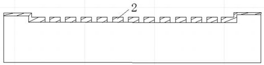
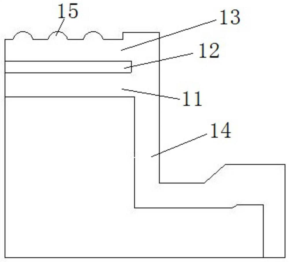
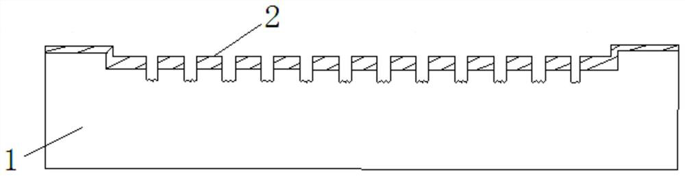
[0030] Such as Figure 1 to Figure 4 As shown, the lower electrode 1 has a sandwich structure. On the upper part of the stainless steel or aluminum base, from bottom to top, there are a first insulating layer 11, a conductive layer 12, and a second insulating layer 13; in addition, there are planes extending from the lower end of the substrate. To the conductive layer DCport (DC power supply terminal), applying a direct current to the DC port will induce a negative charge under the glass. The positive charge of the tungsten layer (conductive layer) and the negative charge under the glas...


PUM


Abstract

The invention discloses a manufacturing method for convex points on the surfaces of lower part electrodes by dry etching. The manufacturing method comprises the following steps that step 1, shield sheets are manufactured according to the distribution and size of the convex points of the lower part electrodes; step 2, the shield sheets are attached to the surfaces of the lower part electrodes, andconcave holes of the lower part electrodes are formed by sandblasting the surfaces of the lower electrodes between the adjacent shield sheets; and step 3, the convex points on the surfaces of the lower part electrodes are easy to form by spraying ceramic powder in the concave holes. Compared with the previous method that masking is carried out, plasma spray is carried out, the concave holes are formed through machining and grinding, then the convex points are bonded, the manufacturing method with the concave points through machining and grinding is faster, more convenient, short in working period, lower in cost and increased in yield.

Description

Technical field [0001] The invention belongs to the technical field of electrode plate regeneration of dry etching equipment, and specifically relates to a manufacturing method for dry etching the surface bumps of the lower electrode. Background technique [0002] The dry etching process technology is currently widely used in the panel and semiconductor industries. In the liquid crystal panel display manufacturing process, dry engraving equipment plays a very important role. Dry etching chamber equipment includes: power supply, air inlet, control unit, upper electrode, lower electrode, cooling gas and vacuum pump. The glass substrate is etched on the lower electrode. The surface of the upper electrode is covered with uniform through-gas holes for evenly distributing the etching gas, and the surface of the lower electrode is equipped with through-holes for introducing helium gas to cool the glass. The glass is adsorbed and fixed by the lower electrode system electrostatic chuck...

Claims


Application Information

Patent Timeline
Patent Type & Authority Patents(China)
IPC IPC(8): C23C4/02C23C4/11G02F1/13C03C15/00
CPCC03C15/00C23C4/02C23C4/11G02F1/1303
Inventor 黄艳芳王慧赵浩
Owner 芜湖通潮精密机械股份有限公司
Why Eureka
Try Eureka