

Pixel defining layer and its preparation raw material and preparation method, display substrate
A technology of pixel defining layer and defining layer, which is applied in the direction of electric solid devices, electrical components, circuits, etc., to achieve the effect of simplifying the preparation process
- Summary
- Abstract
- Description
- Claims
- Application Information
AI Technical Summary
Problems solved by technology
Method used
Image

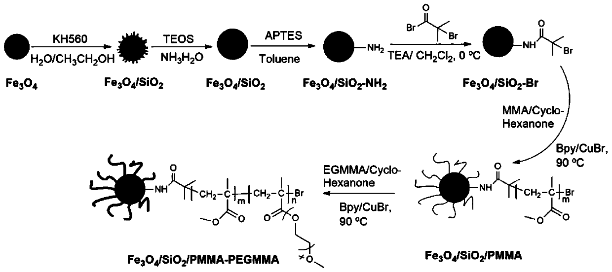


Examples
Embodiment Construction
[0028] In order to make the technical solutions and advantages of the present invention clearer, the embodiments of the present invention will be further described in detail below in conjunction with the accompanying drawings.
[0029] It should be noted that, in the display device, the pixel defining layer includes: a bounding area (also called Bank area), and a pixel area (also called pixel opening area) defined by the bounding area. Wherein, the delimiting area is directly formed by the pixel delimiting layer. In order to solve the current process of preparing the pixel definition layer, it is necessary to use two, or even more than two kinds of raw materials with different affinity and lyophobicity, and to form it through multiple patterning processes, resulting in complicated process and raw material limitations, etc. Problem, the embodiment of the present invention provides a raw material that can be used to prepare the upper lyophobic and lower lyophilic pixel defining ...
PUM
| Property | Measurement | Unit |
|---|---|---|
| magnetic flux density | aaaaa | aaaaa |
Abstract
Description
Claims
Application Information