Microcell resistivity measurement device based on pseudo measured value method, and result display method

A measuring device and resistivity technology, applied in the field of semiconductor measuring devices, to achieve the effects of preventing offset, reducing manufacturing costs, and measuring accurately

Inactive Publication Date: 2019-01-01
HEBEI UNIV OF TECH
View PDF1 Cites 0 Cited by
  • Summary
  • Abstract
  • Description
  • Claims
  • Application Information

AI Technical Summary

Problems solved by technology

The device can solve problems that cannot be solved by the existing technology, and can measure the micro-resistivity of semiconductor silicon wafers in real time, so as to monitor the electrical properties and inhomogeneity of semiconductor silicon wafers

Method used


Image

  • Microcell resistivity measurement device based on pseudo measured value method, and result display method
  • Microcell resistivity measurement device based on pseudo measured value method, and result display method
  • Microcell resistivity measurement device based on pseudo measured value method, and result display method

Examples


Embodiment Construction

[0051] A micro-area resistivity measurement device based on the pseudo-measurement value method and a display method for the results of the present invention will be further described in detail below in conjunction with the accompanying drawings.

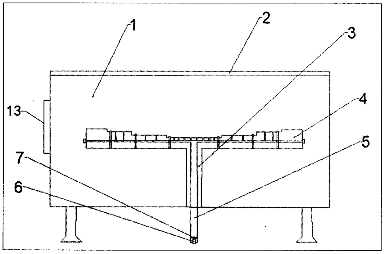
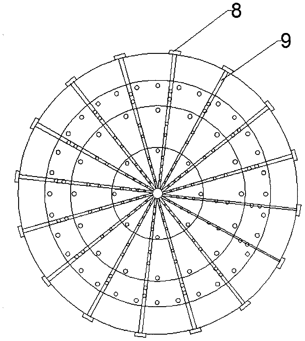
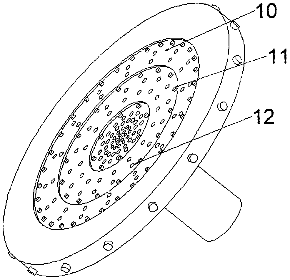
[0052] The present invention is based on a micro-area resistivity measurement device (referred to as the device, attached) based on the pseudo measured value method. Figure 1-3 ), comprising a box body 1, a sealing door 2 arranged on the top of the box body, a test platform column 3 fixed at the center of the bottom of the box body, a test platform 4 fixed at the top of the test platform column, and the The suction pipe 5 connected to the bottom of the test platform column, the motor 6 arranged at the bottom of the suction pipe, the fan blade 7 connected to the motor and fixed in the suction pipe, and the wooden plug fixed on the side of the test platform 8. Radially distributed in the air passage 9, set test slots 10 of different ...


PUM


Abstract

The invention relates to a microcell resistivity measurement device based on a pseudo measured value method, and a result display method. The device comprises a box body, a control system module, a communication module, a sealing door, a test platform column, a test platform, a suction pipe, a motor, a fan blade, a cork, a ventilation duct, a test slot, an electrode, a suction hole, and a liquid crystal display. The test platform does not involve complicated motor control, and the suction force is used to control the contact resistance between a test piece and the electrode, so the measurementis more accurate. The device uses the pseudo measured value method for measurement, and at the same time, is combined with a mobile phone APP, so the measurement is simple and convenient, and more intelligent. A method for displaying the resistivity of a silicon region micro-region can display the uniformity of the resistivity of the sheet to be tested more intuitively, thereby judging whether the sheet to be tested meets industrial requirements or not.

Description

technical field [0001] The invention relates to the technical field of semiconductor measurement devices, in particular to a micro-area resistivity measurement device and a result display method based on a pseudo-measurement value method. Background technique [0002] The electronic information industry based on integrated circuits has become the world's largest industry. The integration level of integrated circuits based on single crystal silicon is getting higher and higher. The diameter of the silicon wafer material is getting larger and larger, while the pattern is getting smaller and smaller, and the size of the circuit is shrinking day by day. All of these put forward stricter requirements on the mechanical and electrical properties of the crystal material. It has important theoretical and practical significance to carry out the test and research on the resistivity distribution of semiconductor materials, especially the research on the electrical characteristics and u...

Claims


Application Information

Patent Timeline
Patent Type & Authority Applications(China)
IPC IPC(8): G01R27/02
CPCG01R27/02
Inventor 刘新福王梦丹李倩文
Owner HEBEI UNIV OF TECH
Why Eureka
Try Eureka