Bias modulation method and system, and plasma processing equipment

A technology of bias voltage modulation and negative bias voltage, which is applied in the direction of discharge tubes, electrical components, circuits, etc., can solve the problem of reducing the attractive force of positive ions, reducing the etching rate of the wafer surface, reducing the number and rate of positive ions reaching the wafer surface, etc. question

Active Publication Date: 2019-01-01
BEIJING NAURA MICROELECTRONICS EQUIP CO LTD
View PDF3 Cites 3 Cited by
  • Summary
  • Abstract
  • Description
  • Claims
  • Application Information

AI Technical Summary

Problems solved by technology

The positive ions accumulated on the wafer surface generate a positive potential, which will reduce the negative bias voltage on the wafer surface, thereby reducing the attraction of the wafer surface to the positive ions in the plasma, reducing the number and rate of positive ions reaching the wafer surface, thereby Reduces the etch rate on the wafer surface, reducing throughput

Method used


Image

  • Bias modulation method and system, and plasma processing equipment
  • Bias modulation method and system, and plasma processing equipment
  • Bias modulation method and system, and plasma processing equipment

Examples


Embodiment 1

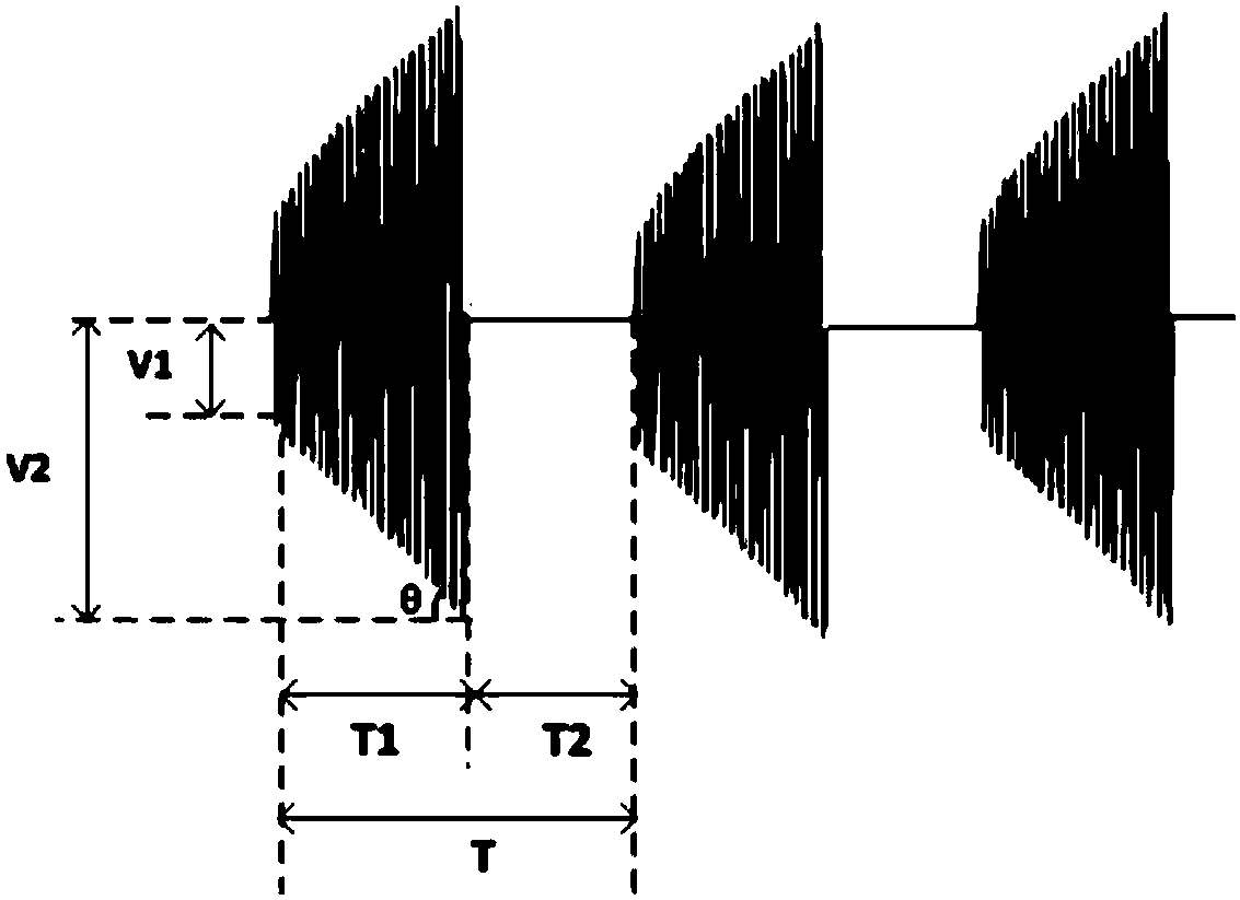
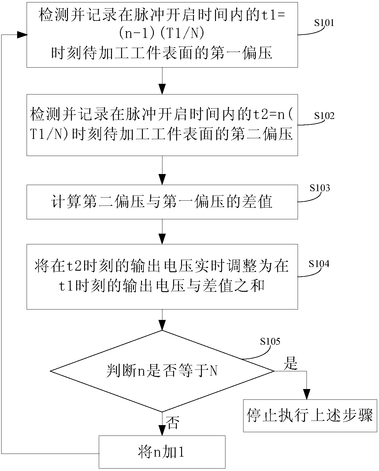
[0051] This embodiment provides a method for modulating the bias voltage on the surface of the workpiece to be processed. The bias power generated by the bias RF source is loaded on the base carrying the workpiece to be processed, so that the surface of the workpiece placed on the base to be processed Generate a negative bias voltage. During the bias power loading period, the voltage generated by the bias RF source increases from the initial voltage to the target voltage to compensate for the negative bias voltage lost on the surface of the workpiece to be processed, so that the negative bias voltage on the surface of the workpiece to be processed is The preset range is maintained during bias power loading.

[0052] Among them, the preset range refers to that after the bias power is loaded on the surface of the workpiece to be processed, it can ensure that the positive ions reaching the surface of the workpiece to be processed have a certain amount and rate, thereby ensuring th...

Embodiment 2

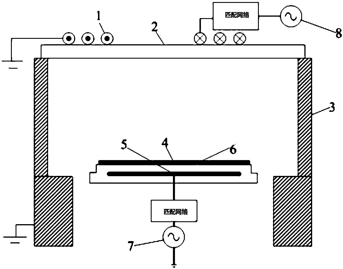
[0075] This embodiment provides a bias modulation system, such as Figure 5 As shown, it is used to modulate the negative bias voltage of the workpiece to be processed placed on the surface of the base 10, including: a bias RF source 7, the bias RF source 7 is electrically connected to the base 10 carrying the workpiece to be processed, for A bias power is applied to the base 10 to generate a negative bias on the surface of the workpiece to be processed. The voltage adjustment module 9, the voltage adjustment module 9 is electrically connected to the bias RF source 7, and is used to increase the voltage generated by the bias RF source 7 from the initial voltage to the target voltage during bias power loading, so as to compensate the surface of the workpiece to be processed Loss of negative bias voltage, so that the negative bias voltage of the surface of the workpiece to be processed is kept within the preset range.

[0076] The voltage adjustment module 9 can make the increa...

Embodiment 3

[0086] This embodiment provides a plasma processing device, including a base for carrying workpieces to be processed, a plasma generating device, and the bias modulation system in Embodiment 2, where the bias modulation system is electrically connected to the base.

[0087] Wherein, the plasma generating device includes a coil and an upper electrode radio frequency source connected thereto, and the upper electrode radio frequency source is a continuous wave radio frequency source or a pulse modulation radio frequency source.

[0088] By adopting the bias voltage modulation system in Embodiment 2, the plasma processing equipment can reduce or avoid the loss of negative bias voltage on the surface of the workpiece to be processed, thereby reducing or avoiding the loss of plasma energy bombarded to the surface of the workpiece to be processed , so that the processing rate of the processed workpiece is kept within the preset range, on the one hand, the productivity of the processed...


PUM


Abstract

The invention provides a bias modulation method and system, and plasma processing equipment. The method is to load the bias power generated by a bias radio frequency source on a pedestal bearing a to-be-processed workpiece so that negative bias can be generated on the surface of the to-be-processed workpiece placed on the pedestal; and during the loading of the bias power, voltage generated by thebias radio frequency source can be increased to target voltage from initial voltage to compensate for the losing negative bias on the surface of the to-be-processed workpiece, so that the negative bias on the surface of the to-be-processed workpiece can be maintained in a preset range during the loading of the bias power. The bias modulation system is also disclosed. The disclosed plasma processing equipment includes the bias modulation system. The bias modulation method and system and the plasma processing equipment can maintain the negative bias on the surface of the to-be-processed workpiece in the preset range, so that the technology rate (such as etching rate or deposition rate) of the to-be-processed workpiece can be maintained in the preset range.

Description

technical field [0001] The invention relates to the field of semiconductors, in particular to a bias voltage modulation method, a bias voltage modulation system and plasma processing equipment. Background technique [0002] With the rapid development of the manufacturing process of semiconductor components, the requirements for the performance and integration of components are getting higher and higher, which makes plasma technology widely used. In the plasma etching or deposition system, by introducing various reactive gases (such as Cl 2 ,SF 6 ,C 4 f 8 ,O 2 etc.), use an external electromagnetic field (DC or AC) to make the bound electrons in the gas atoms get rid of the potential well and become free electrons, and the free electrons that have gained kinetic energy collide with molecules, atoms or ions to completely dissociate the gas and form a plasma. Plasma contains a large number of active particles such as electrons, ions (including positive ions and negative io...

Claims


Application Information

Patent Timeline
Patent Type & Authority Applications(China)
IPC IPC(8): H01J37/32
CPCH01J37/321H01J2237/3348H01J37/32
Inventor 苏恒毅韦刚
Owner BEIJING NAURA MICROELECTRONICS EQUIP CO LTD
Why Eureka
Try Eureka