Semiconductor device and forming method thereof

A semiconductor and device technology, applied in the field of semiconductor devices and their formation, can solve problems such as poor performance of semiconductor devices, and achieve the effects of enhanced etching resistance, low loss and improved performance

Active Publication Date: 2019-01-04
SEMICON MFG INT (SHANGHAI) CORP +1
View PDF4 Cites 4 Cited by
  • Summary
  • Abstract
  • Description
  • Claims
  • Application Information

AI Technical Summary

Problems solved by technology

[0004] However, the performance of semiconductor devices formed us

Method used


Image

  • Semiconductor device and forming method thereof
  • Semiconductor device and forming method thereof
  • Semiconductor device and forming method thereof

Examples


Embodiment Construction

[0031] As described in the background art, the semiconductor device formed by the prior art has poor performance.

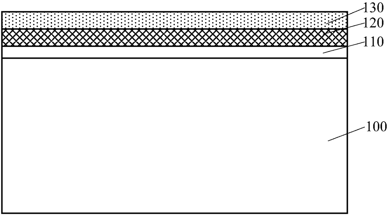
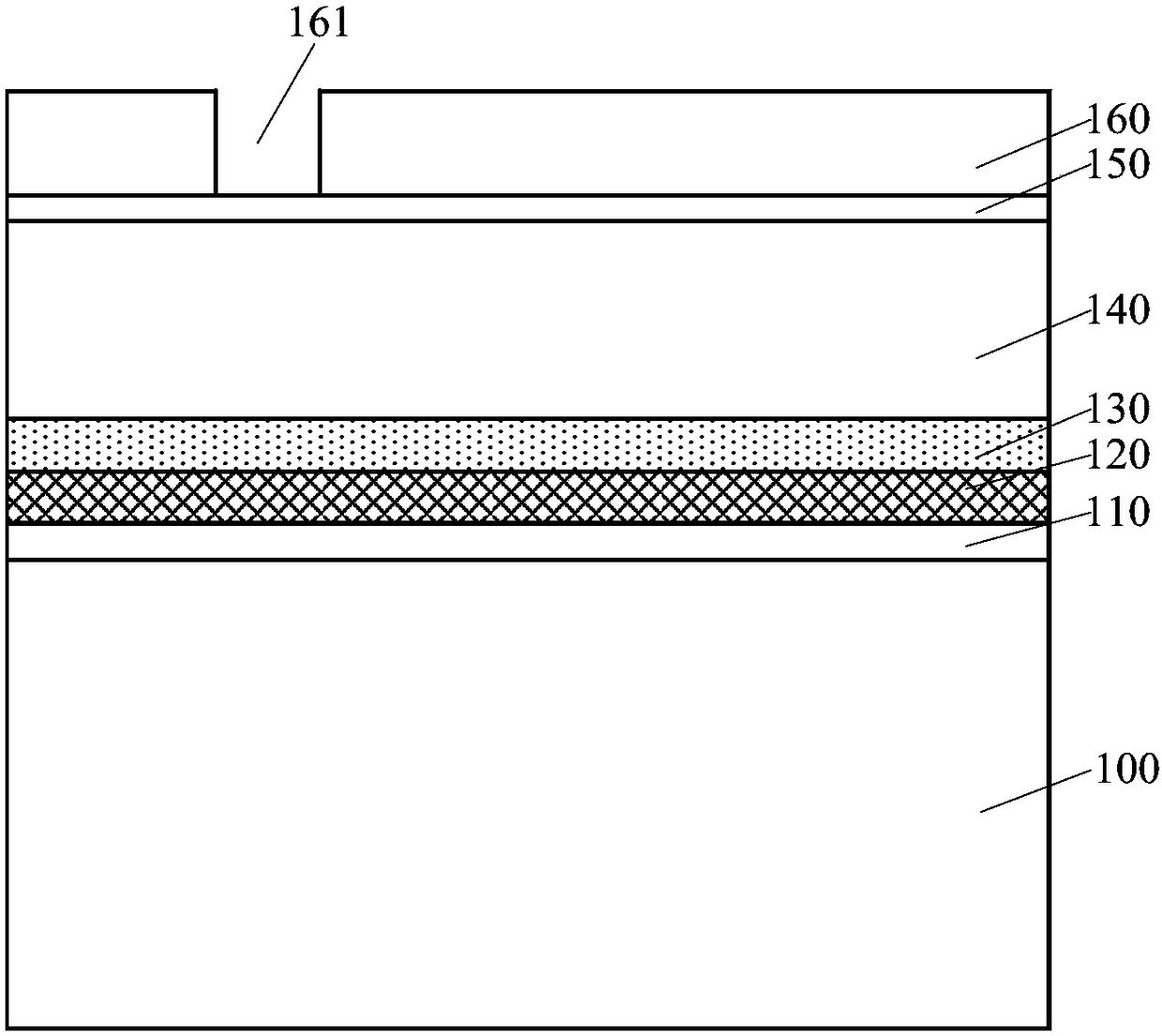
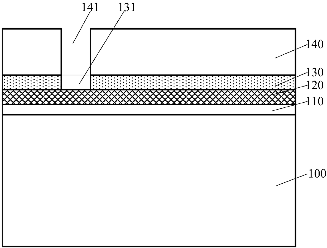
[0032] A method for forming a semiconductor device includes: providing a material layer to be etched, the material layer to be etched is provided with a top mask layer, and the material of the top mask layer is silicon oxycarbide; on the top mask layer A first opening penetrating through the top mask layer is formed; after forming the first opening, an intermediate patterning process is performed; after the intermediate patterning process is performed, a second opening penetrating through the top mask layer is formed in the top mask layer, The second opening and the first opening are separated from each other.

[0033] However, the performance of the semiconductor device formed by the above-mentioned method is poor, and it is found through research that the reasons are:

[0034] The first opening and the second opening are used to jointly form the target pattern in the...


PUM


Abstract

The invention provides a semiconductor device and a forming method thereof. The method includes providing a material layer to be etched, wherein the material layer to be etched is provided with a toplayer mask layer; forming a first opening running through the top layer mask layer in the top layer mask layer, the sidewall material of the first opening having a first density; performing a first surface treatment process on the sidewall of the first opening such that the sidewall material of the first opening has a second density, the second density being greater than the first density; performing an intermediate patterning process after the first surface treatment process; and after performing the intermediate patterning process, forming a second opening running through the top layer masklayer in the top layer mask layer, the second opening and the first opening being separated from each other. The method improves the performance of the semiconductor device.

Description

Technical field [0001] The invention relates to the field of semiconductor manufacturing, in particular to a semiconductor device and a method of forming the same. Background technique [0002] In the process of manufacturing semiconductor devices, photolithography is usually used to transfer the pattern on the mask to the substrate. The photolithography process includes: providing a substrate; forming a photoresist layer on the substrate; exposing and developing the photoresist layer to form a patterned photoresist layer; using the patterned photoresist layer as a mask The film etches the substrate so that the pattern on the photoresist layer is transferred to the substrate; the photoresist layer is removed. As the size of semiconductor devices continues to shrink, the critical dimensions of lithography are gradually approaching or even exceeding the physical limits of lithography, which poses more severe challenges to lithography technology. The basic idea of ​​the double pat...

Claims


Application Information

Patent Timeline
IPC IPC(8): H01L21/033
CPCH01L21/0334H01L21/0337
Inventor 王士京姚达林张海洋
Owner SEMICON MFG INT (SHANGHAI) CORP
Why Eureka
Try Eureka