A memory and a forming method thereof, and a semiconductor device

A memory and storage node technology, applied in semiconductor devices, semiconductor/solid-state device manufacturing, electric solid-state devices, etc., can solve the problem of large contact resistance of bit line contact and bit line contact area storage node contact and storage node contact area, preparation high cost

Active Publication Date: 2019-01-04
CHANGXIN MEMORY TECH INC
View PDF4 Cites 19 Cited by
  • Summary
  • Abstract
  • Description
  • Claims
  • Application Information

AI Technical Summary

Problems solved by technology

[0006] The purpose of the present invention is to provide a method for forming a memory, so as to solve the problem that in the existing method of forming, multiple photolithography processes are required, which not only makes the preparation cost higher, but also easily produces displacement deviation, which in turn leads to bit line contact. The problem of large contact resistance between the contact area of ​​the bit line and the contact area of ​​the storage node and the contact area of ​​the storage node

Method used


Image

  • A memory and a forming method thereof, and a semiconductor device
  • A memory and a forming method thereof, and a semiconductor device
  • A memory and a forming method thereof, and a semiconductor device

Examples


Embodiment 1

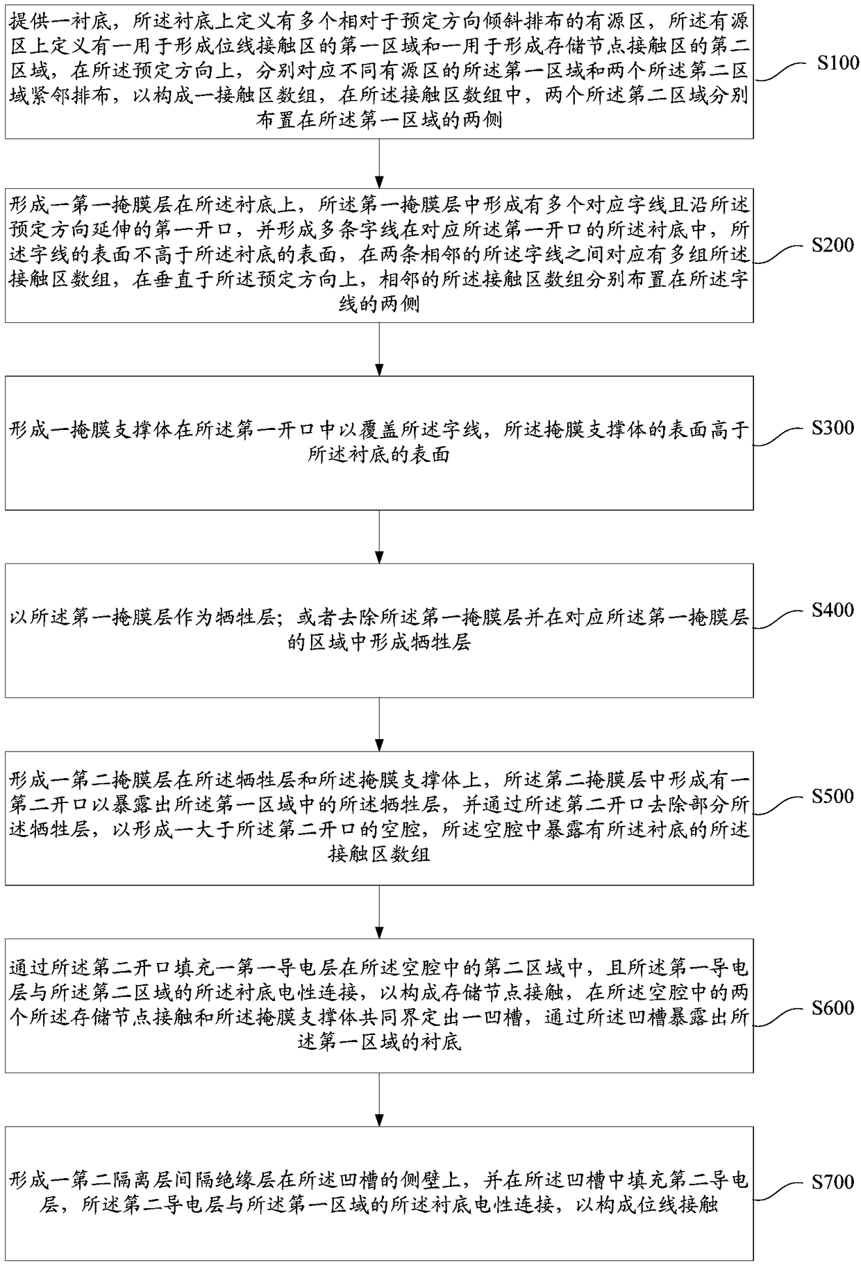
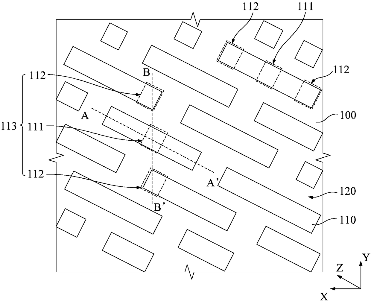
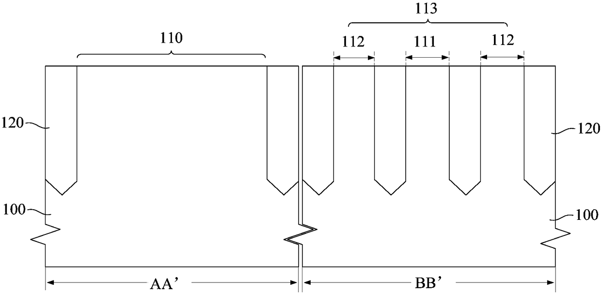
[0120] Figure 2a A top view of the memory forming method in Embodiment 1 of the present invention when step S100 is executed; Figure 2b for Figure 2a The shown cross-sectional views of the memory forming method in Embodiment 1 of the present invention along the directions AA' and BB' when step S100 is executed.

[0121] In step S100, combining Figure 2a and Figure 2b As shown, a substrate 100 is provided, and the substrate 100 is defined with a plurality of active regions 110 arranged obliquely with respect to a predetermined direction, and a first active region 110 is defined on the active region 110 for forming a bit line contact region. A region 111 and a second region 112 for forming a storage node contact region. In the predetermined direction (Y direction), one first region 111 and two second regions 112 respectively corresponding to different active regions 110 are arranged adjacent to each other to form a contact region array 113 . In the array of contact reg...

Embodiment 2

[0185] Figure 9a is a top view of the memory in Embodiment 2 of the present invention, Figure 9b for Figure 9a Shown are cross-sectional views of the memory in Embodiment 2 of the present invention along the directions AA' and BB'. Such as Figure 9a and Figure 9b As shown, the memory includes:

[0186] A substrate 100, on which are defined a plurality of active regions 110 arranged obliquely (Z direction) relative to a predetermined direction and isolation structures 120 between the active regions, the active regions 110 is formed with a bit line contact region 111a and at least one storage node contact region 112a. In the predetermined direction (Y direction), the bit line contact region 111a and two storage node contact regions corresponding to different active regions 110 are respectively The regions 111b are arranged adjacent to each other to form a contact region array 113a. In the contact region array 113a, the two storage node contact regions 112a are respecti...

Embodiment 3

[0201] Based on the core idea of ​​the invention, the invention also provides a semiconductor device. Those skilled in the art know that in the field of semiconductors, most devices need to use lead-out terminals to lead out corresponding lead-out areas, so that corresponding functions of the devices can be realized through electrical control. In addition, in semiconductor devices, there are usually multiple lead-out regions. To ensure the performance of the device, different kinds of lead-out regions need to be isolated from each other. Therefore, the present invention provides a semiconductor device based on the core idea of ​​"self-alignment and self-truncation".

[0202] Figure 10a is a top view of the semiconductor device in Embodiment 3 of the present invention, Figure 10b for Figure 10a A schematic diagram of the distribution of the first contact region and the second contact region in the semiconductor device in the third embodiment of the present invention is sh...


PUM


Abstract

The invention provides a memory and a forming method thereof, and a semiconductor device. A mask support and a sacrificial layer are formed in self-alignment with a first mask layer corresponding to aword line pattern, a cavity is formed in self-alignment with a second mask layer, so as to define a region in which the memory node contact and the bit line contact are formed, so that the memory node contact and the bit line contact can be sequentially formed in the cavity under the action of an isolation barrier of the mask support and the sacrificial layer. That is, in the process of forming the storage node contact and the bit line contact, By using only one photolithography process, the execution times of the photolithography process are reduced, the problem of large displacement deviation due to multiple photolithography processes is avoided, and the contact resistance between the memory node contact and the memory node contact region, and between the bit line contact and the bit line contact region can be reduced.

Description

technical field [0001] The invention relates to the technical field of semiconductors, in particular to a memory, a method for forming the same, and a semiconductor device. Background technique [0002] A memory typically includes a storage capacitor for storing charge representing stored information and a storage transistor connected to the storage element. An active region, a drain region, and a gate are formed in the memory transistor, the gate is used to control the flow of current between the source region and the drain region, and is connected to a word line, and the source region is used to form a bit A line contact region is used to connect to a bit line, and the drain region is used to form a storage node contact region to connect to a storage capacitor. [0003] Usually, after the word line is formed, a bit line contact needs to be formed on the bit line contact area, and then connected to the bit line through the bit line contact, and a storage node contact area ...

Claims


Application Information

Patent Timeline
Patent Type & Authority Applications(China)
IPC IPC(8): H01L21/8242H01L27/108
CPCH10B12/30H10B12/0335H10B12/485
Inventor 不公告发明人
Owner CHANGXIN MEMORY TECH INC
Why Eureka
Try Eureka