Trench gate MOSFET and manufacturing method thereof

A manufacturing method and trench gate technology, applied in semiconductor/solid-state device manufacturing, electrical components, circuits, etc., can solve the problems of reduced device performance, poor current path uniformity, etc., to achieve uniform current path, improve breakdown voltage, improve The effect of pressure resistance

Inactive Publication Date: 2019-01-04
SHANGHAI HUAHONG GRACE SEMICON MFG CORP
View PDF4 Cites 6 Cited by
  • Summary
  • Abstract
  • Description
  • Claims
  • Application Information

AI Technical Summary

Problems solved by technology

However, in the existing structure, due to the deep depth of the trench 111b, the devices are all edge breakdown, and the un

Method used


Image

  • Trench gate MOSFET and manufacturing method thereof
  • Trench gate MOSFET and manufacturing method thereof
  • Trench gate MOSFET and manufacturing method thereof

Examples


Embodiment Construction

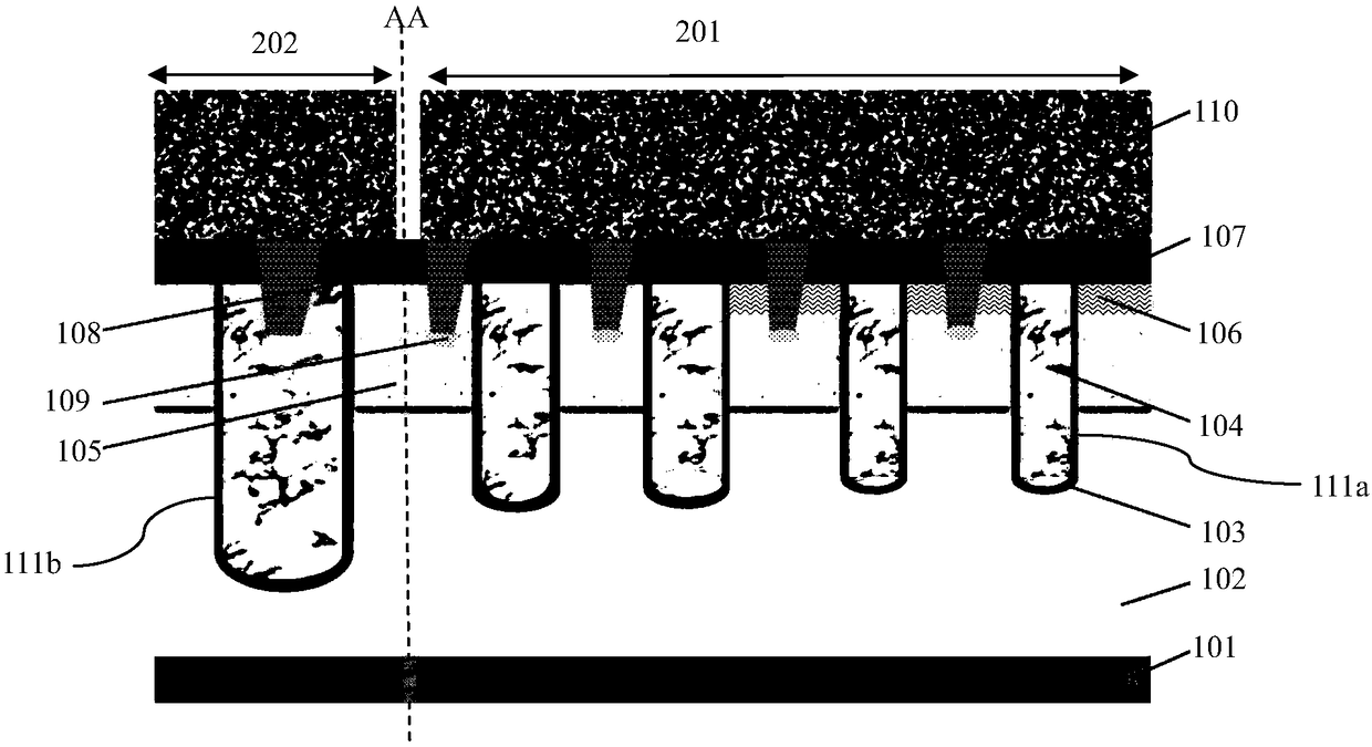
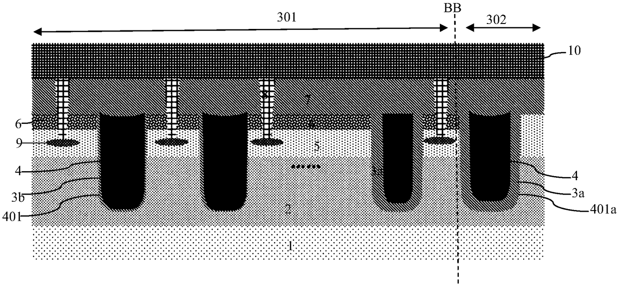
[0058] like figure 2 As shown, it is a schematic structural diagram of a trench gate MOSFET according to an embodiment of the present invention. The trench gate MOSFET according to this embodiment of the present invention includes an inner region and an edge region, figure 2 In the sectional view of , the inner area and the edge area are separated by a dotted line BB, the inner area is indicated by a mark 301 , and the edge area is indicated by a mark 302 . The inner region is the conduction region of the trench gate MOSFET, which is composed of a plurality of primitive cells arranged periodically; the edge region is located at the edge of the conduction region, and is used to connect the primitive cells in the conduction region The gate structure leads out.

[0059] Both the drift region 2 of the first conductivity type and the body region 5 of the second conductivity type are formed in the inner region and the edge region, and the body region 5 is located on the surface o...


PUM


Abstract

The invention discloses a trench gate MOSFET, comprising an inner region and an edge region, wherein the edge region is located at the edge of the conduction region for leading out the gate structureof each cell in the conduction region; A first trench is formed in the inner region, and a second trench having a width equal to or greater than the first trench is formed in the edge region. Forminga first gate dielectric layer on the inner side surface of each first trench, and forming a second gate dielectric layer having a thickness greater than the first gate dielectric layer on the inner side surface of the second trench; Each of the first and second trenches is filled with a polysilicon gate, and each polysilicon gate is connected to the gate through a contact hole formed in the top ofthe polysilicon gate of the second trench. The invention also discloses a manufacturing method of a trench gate MOSFET. The invention can improve the withstand voltage ability of the edge region andcause the breakdown of the device to occur in the inner region, thereby improving the shock resistance of the device.

Description

technical field [0001] The invention relates to the field of manufacturing semiconductor integrated circuits, in particular to a trench gate MOSFET. The invention also relates to a manufacturing method of the trench gate MOSFET. Background technique [0002] like figure 1 Shown is a schematic diagram of the structure of the existing trench gate MOSFET; the existing trench gate MOSFET includes an inner region and an edge region, figure 1 In the sectional view of , the inner area and the edge area are separated by a dotted line AA, the inner area is indicated by a mark 201 , and the edge area is indicated by a mark 202 . The inner region is the conduction region of the trench gate MOSFET, which is composed of a plurality of primitive cells arranged periodically; the edge region is located at the edge of the conduction region, and is used to connect the primitive cells in the conduction region The gate structure is derived; the device structure of the existing trench gate MO...

Claims


Application Information

Patent Timeline
IPC IPC(8): H01L29/78H01L29/423H01L21/336
CPCH01L29/4236H01L29/66666H01L29/7827H01L29/7831
Inventor 石磊
Owner SHANGHAI HUAHONG GRACE SEMICON MFG CORP
Why Eureka
Try Eureka