Method for preparing large-size CVD (Chemical Vapor Deposition) diamond crystal

A diamond single crystal and diamond technology, applied in the field of diamond wafer preparation, can solve problems such as polycrystalline and poor crystal quality, and achieve the effects of ensuring crystal quality, ensuring crystal growth orientation, and inhibiting growth defects

Inactive Publication Date: 2019-01-08
JINAN ZHONGWU NEW MATERIALS CO LTD
View PDF7 Cites 18 Cited by
  • Summary
  • Abstract
  • Description
  • Claims
  • Application Information

AI Technical Summary

Problems solved by technology

[0007] The present invention provides a method for preparing large-size CVD diamond crystals. The CVD method is used to grow large-size diamond crystals on spliced ​​HPHT diam...

Method used


Image

  • Method for preparing large-size CVD (Chemical Vapor Deposition) diamond crystal
  • Method for preparing large-size CVD (Chemical Vapor Deposition) diamond crystal
  • Method for preparing large-size CVD (Chemical Vapor Deposition) diamond crystal

Examples


Embodiment Construction

[0033] The manufacture method of large-scale semiconductor diamond wafer in the present invention mainly comprises the following steps:

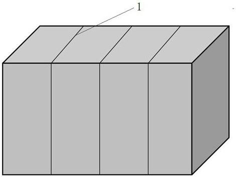
[0034] 1. Cut the diamond single crystal grown by the HPHT method into multiple slices along the same direction, and the cutting seam 1 is as figure 1 As shown, after the cutting is completed, the surface is polished and processed to form a rectangular or square HPHT diamond single crystal wafer, which is used as a seed crystal for MPCVD diamond growth;

[0035] 2. Clean the surface of the HPHT diamond single crystal wafer. Specifically, treat the sample with aqua regia (concentrated hydrochloric acid: nitric acid = 3:1) at 55°C-65°C for 10 minutes, and then sonicate with acetone at room temperature for 10-15 minutes;

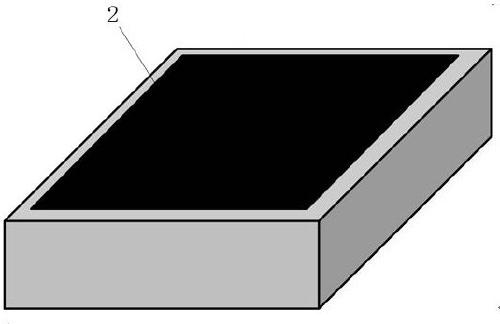
[0036] 3. If figure 2 As shown, the photoresist 2 is cast on the HPHT diamond single crystal wafer, and the hard film is baked for 30-60 minutes; the design pattern is formed after exposure by a photolithography machine.

...


PUM

PropertyMeasurementUnit
Widthaaaaaaaaaa
Thicknessaaaaaaaaaa

Abstract

The invention discloses a method for preparing a large-size CVD (Chemical Vapor Deposition) diamond crystal. The method comprises the following steps: (1) cutting a single diamond crystal grown by using an HPHT (High Temperature and High Pressure) method so as to obtain single HPHT diamond crystal sheets; (2) carrying out surface cleaning; (3) throwing a photoresist to the single HPHT diamond crystal sheets, and carrying out membrane hardening so as to obtain design patterns; (4) depositing a medium membrane by using a CVD method; (5) removing the photoresist and the medium membrane outside the design patterns so as to obtain design medium membrane patterns; (6) splicing the single HPHT diamond crystal sheets in CVD equipment, and carrying out plasma etching so as to obtain a new surface;(7) growing a thick-layer CVD single diamond crystal on the new surface by using a microwave plasma chemical vapor deposition method; (8) cutting and removing the spliced single HPHT diamond crystal sheets, thereby obtaining the self-supported large-size CVD diamond crystal. By adopting the method, growth defects at crystal boundaries and parts nearby of spliced single diamond crystals grown by using the CVD method can be avoided, the quality of the crystal can be ensured, and the self-supported large-size CVD diamond crystal can be prepared.

Description

technical field [0001] The invention relates to a method for preparing a large-size, low-defect diamond wafer, belonging to the technical field of crystal growth. Background technique [0002] Diamond wafer preparation mainly includes high temperature and high pressure method (HPHT) and microwave plasma chemical vapor deposition (MPCVD). Synthesizing diamond by HPHT requires the use of a metal catalyst, and its atoms will inevitably penetrate into the diamond crystal and exist in the form of impurities, which will affect its purity. At present, the maximum size of large-grain diamond single crystal wafers grown by high-temperature and high-pressure methods has reached more than 10 mm, which is still far from the requirements of semiconductor epitaxy. However, high-quality diamond single crystals grown by MPCVD can be completely colorless and transparent, with almost no impurities. At present, the maximum size of CVD diamond has reached 12.5mm, and mosaic splicing has reach...

Claims


Application Information

Patent Timeline
IPC IPC(8): C30B29/04C30B25/20
CPCC30B25/186C30B25/205C30B29/04
Inventor 刘长江王笃福王希玮王盛林
Owner JINAN ZHONGWU NEW MATERIALS CO LTD
Why Eureka
Try Eureka