

Semiconductor avalanche failure analysis and testing method and device based on thermal imaging technology
A thermal imaging technology and failure analysis technology, which is applied in the field of robustness of power semiconductors and can solve the problem of not being able to observe the transfer of hot spots inside the device.
- Summary
- Abstract
- Description
- Claims
- Application Information
AI Technical Summary
Problems solved by technology
Method used
Image

Examples
Embodiment 1
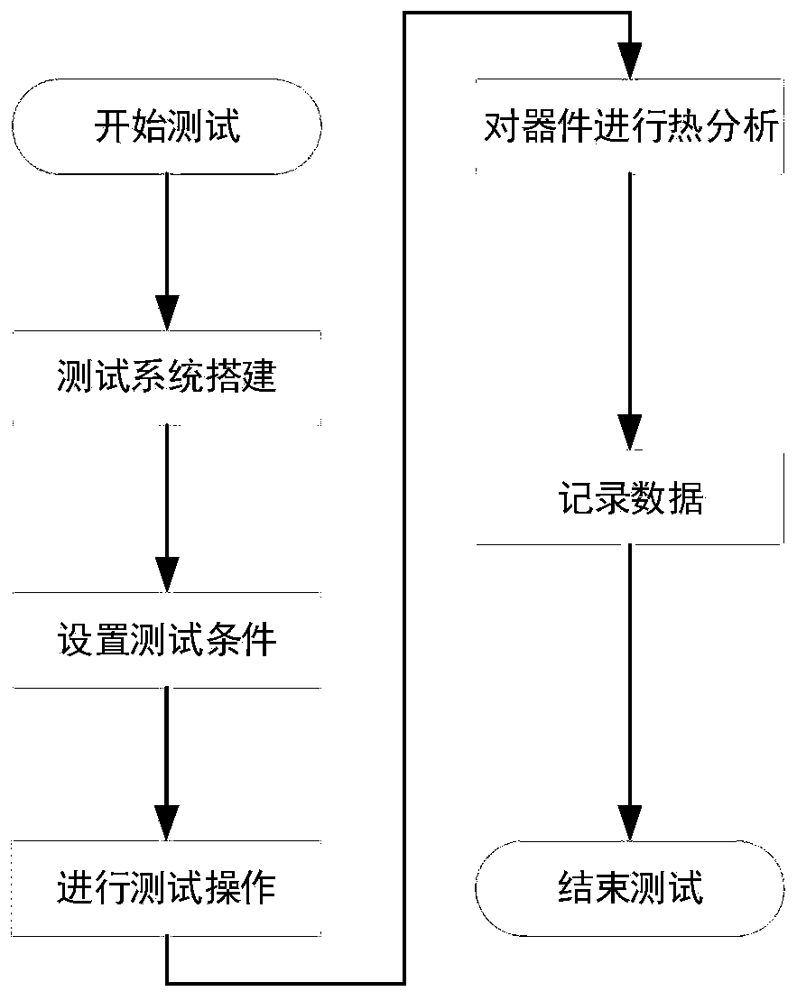
[0024] A test method for semiconductor avalanche failure analysis based on thermal imaging technology, comprising the following test steps:
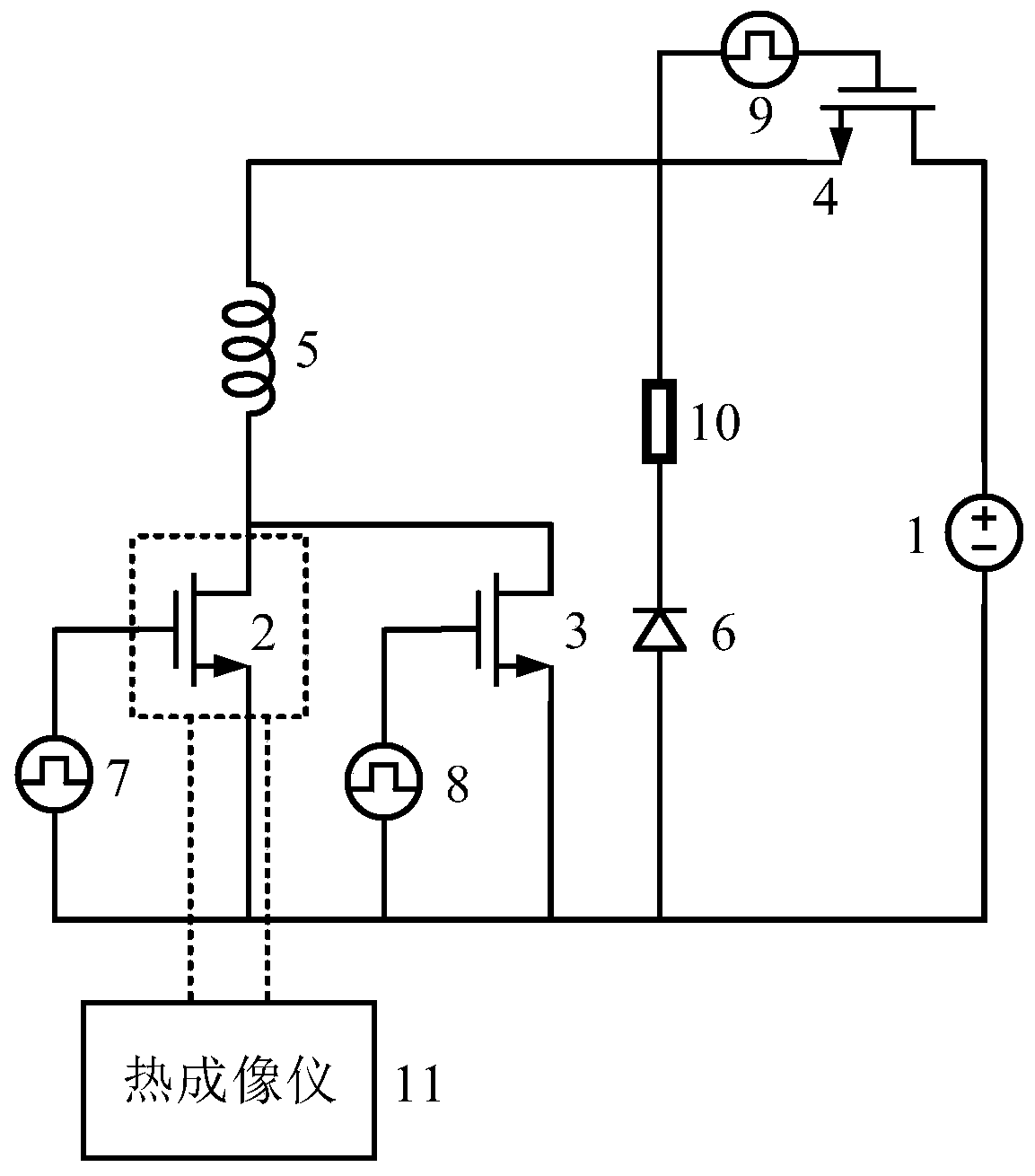
[0025] a) Test system construction: the system includes a DC voltage source 1 and a thermal imager 11, the positive pole of the DC voltage source 1 is connected to a power switching device 4 and is connected to the drain of the power switching device 4, and the negative pole of the DC voltage source 1 is connected There are a power device 2 to be tested, a short-circuit power device 3 and a freewheeling diode 6, and the negative pole of the DC voltage source 1 is connected to the source of the power device 2 to be tested, the source of the short-circuited power device 3 and the anode of the freewheeling diode 6 , the cathode of the freewheeling diode 6 is connected to a power resistor 10 and is connected to one end of the power resistor 10, and the other end of the power resistor 10 is connected to the gate of the power switching device 4...
Embodiment 2
[0031] A semiconductor avalanche failure analysis and testing device based on thermal imaging technology, including a DC voltage source 1 and a thermal imager 11, the anode of the DC voltage source 1 is connected to a power switching device 4 and connected to the drain of the power switching device 4, and the DC The negative pole of the voltage source 1 is connected to the power device 2 to be tested, the short-circuit power device 3 and the freewheeling diode 6, and the negative pole of the DC voltage source 1 is connected to the source of the power device 2 to be tested, the source of the short-circuit power device 3 and the freewheeling diode 6. The anode of the freewheeling diode 6 is connected, the cathode of the freewheeling diode 6 is connected with a power resistor 10 and connected with one end of the power resistor 10, and the other end of the power resistor 10 is connected to the gate of the power switching device 4 through the third pulse voltage source 9, to be The ...
PUM
 Abstract
Description
Claims
Application Information