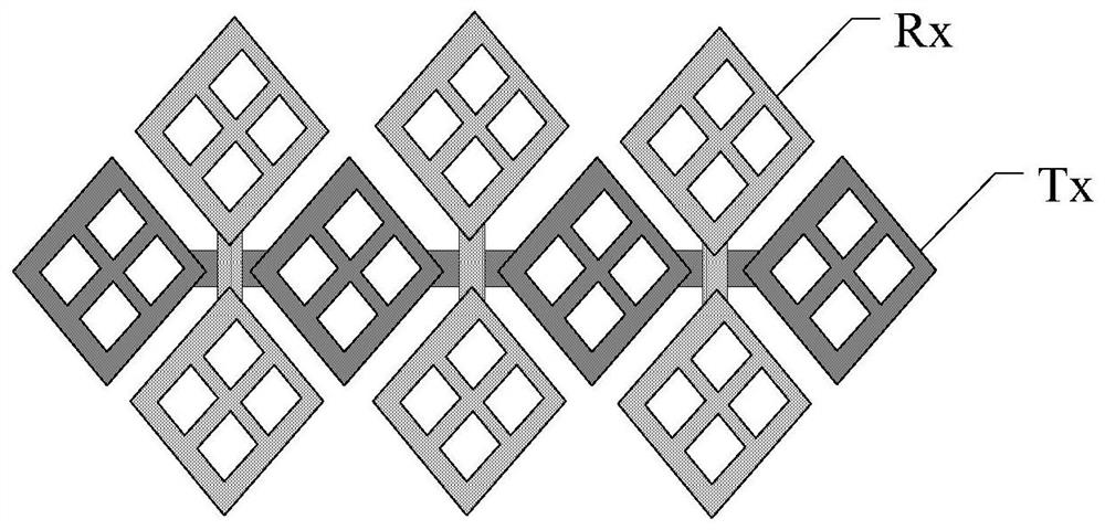
A touch display panel, manufacturing method thereof, and display device
A touch display panel and encapsulation layer technology, which is applied in the fields of instruments, computing, electrical digital data processing, etc., can solve the problems of lower touch resolution, fewer driving electrodes and sensing electrodes, and low utilization rate of touch display panels.
- Summary
- Abstract
- Description
- Claims
- Application Information
AI Technical Summary
Problems solved by technology
Method used
Image
Examples
Embodiment 1
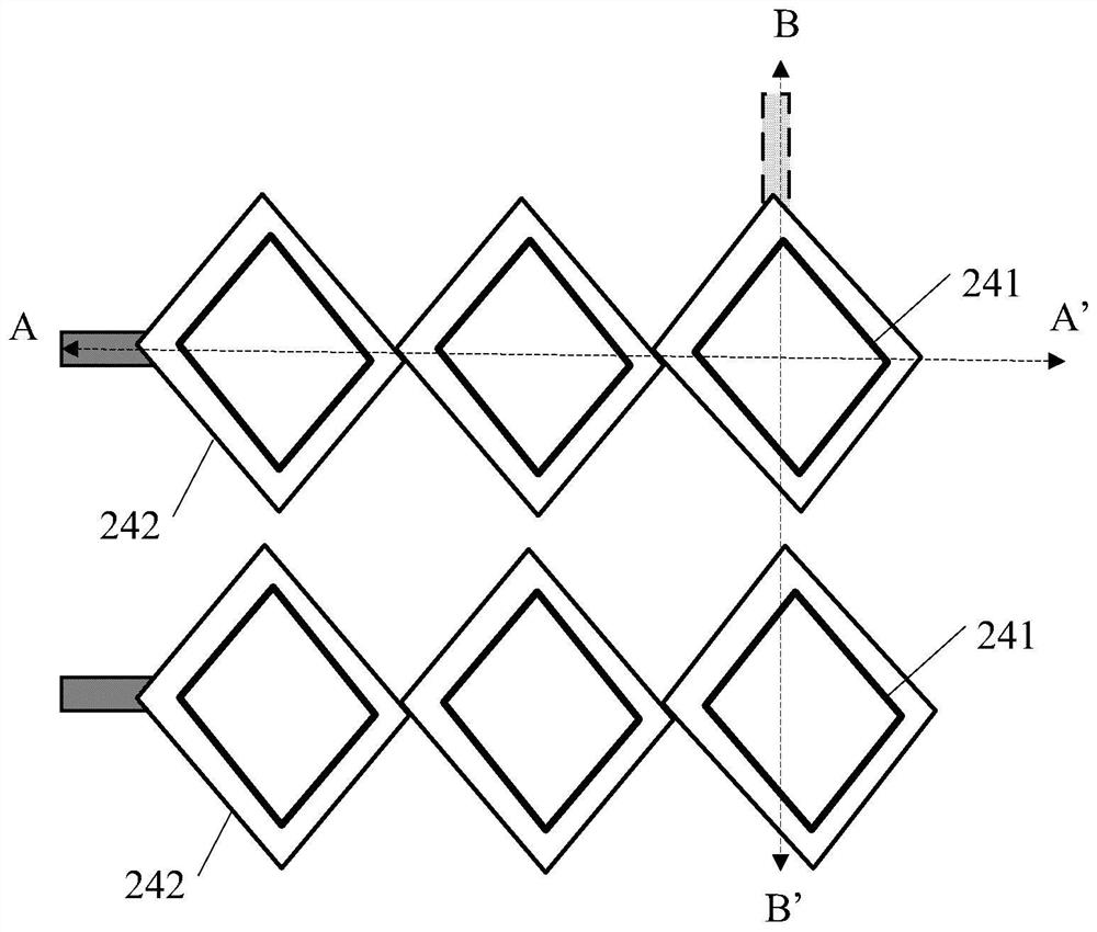
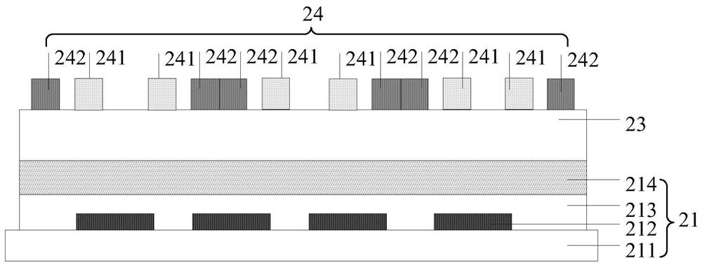
[0048] refer to figure 2 , showing a schematic structural view of a touch display panel according to an embodiment of the present invention, image 3 show figure 2 The sectional view of the shown touch display panel along section A-A', Figure 4 show figure 2 The shown cross-sectional view of the touch display panel along section B-B'.
[0049] An embodiment of the present invention provides a touch display panel, including: a substrate 21, an electrode connection layer 22 formed on the substrate 21; a first insulating layer 23, the first insulating layer 23 covering the electrode connection layer 22, formed on the The electrode layer 24 on the first insulating layer 23 .
[0050] Wherein, the electrode layer 24 includes a plurality of first electrodes 241 and a plurality of second electrodes 242, such as figure 2 As shown, both the first electrode 241 and the second electrode 242 are in a ring-shaped closed structure, and the second electrode 242 surrounds the first ...
Embodiment 2
[0070] refer to Figure 6 , which shows a flow chart of a method for manufacturing a touch display panel according to an embodiment of the present invention, which may specifically include the following steps:
[0071] Step 601, providing a substrate.
[0072] In the embodiment of the present invention, when manufacturing the touch display panel, a substrate 21 needs to be provided first.
[0073] Specifically, a light-emitting device is formed on a base; an encapsulation layer is formed, and the encapsulation layer covers the light-emitting device; and a second insulating layer is formed on the encapsulation layer.
[0074] refer to Figure 7 , shows a schematic structural view of the substrate formed in the embodiment of the present invention.
[0075] Firstly, an anode is formed on the substrate 211, then a light-emitting layer is formed on the anode by evaporation or printing, and finally a cathode is formed to realize the formation of the light-emitting device 212 on t...
Embodiment 3
[0098] An embodiment of the present invention provides a display device, including the above-mentioned touch display panel.
[0099] Of course, the display device also includes a driving chip, which is respectively connected to the first electrode 241 and the second electrode 242 in the electrode layer 24. When the first electrode 241 is the sensing electrode Rx and the second electrode 242 is the driving electrode Tx, It is used to provide a detection signal to the second electrode 242 in the electrode layer 24 and receive a signal from the first electrode 241 in the electrode layer 24 to calculate the user's touch position; or, when the first electrode 241 is a driving electrode Tx, the second electrode When the second electrode 242 is the sensing electrode Rx, it is used to provide a detection signal to the first electrode 241 in the electrode layer 24 and receive a signal from the second electrode 242 in the electrode layer 24 to calculate the user's touch position.
[010...
PUM
 Abstract
Description
Claims
Application Information
 - R&D
- Intellectual Property
- Life Sciences
- Materials
- Tech Scout
- Unparalleled Data Quality
- Higher Quality Content
- 60% Fewer Hallucinations
Browse by: Latest US Patents, China's latest patents, Technical Efficacy Thesaurus, Application Domain, Technology Topic, Popular Technical Reports.
© 2025 PatSnap. All rights reserved.Legal|Privacy policy|Modern Slavery Act Transparency Statement|Sitemap|About US| Contact US: help@patsnap.com


