A through-hole manufacturing method, an array substrate manufacturing method and an array substrate

A manufacturing method and array substrate technology, applied in the field of array substrates, can solve problems such as high cost and complicated manufacturing process, and achieve the effect of reducing manufacturing cost and simplifying the manufacturing process

Active Publication Date: 2019-01-15
SOUTH CHINA UNIV OF TECH
View PDF3 Cites 4 Cited by
  • Summary
  • Abstract
  • Description
  • Claims
  • Application Information

AI Technical Summary

Problems solved by technology

The production of each via needs to adopt the standard yellow light process, the production process is complicated and the cost is high

Method used


Image

  • A through-hole manufacturing method, an array substrate manufacturing method and an array substrate
  • A through-hole manufacturing method, an array substrate manufacturing method and an array substrate
  • A through-hole manufacturing method, an array substrate manufacturing method and an array substrate

Examples


Embodiment 1

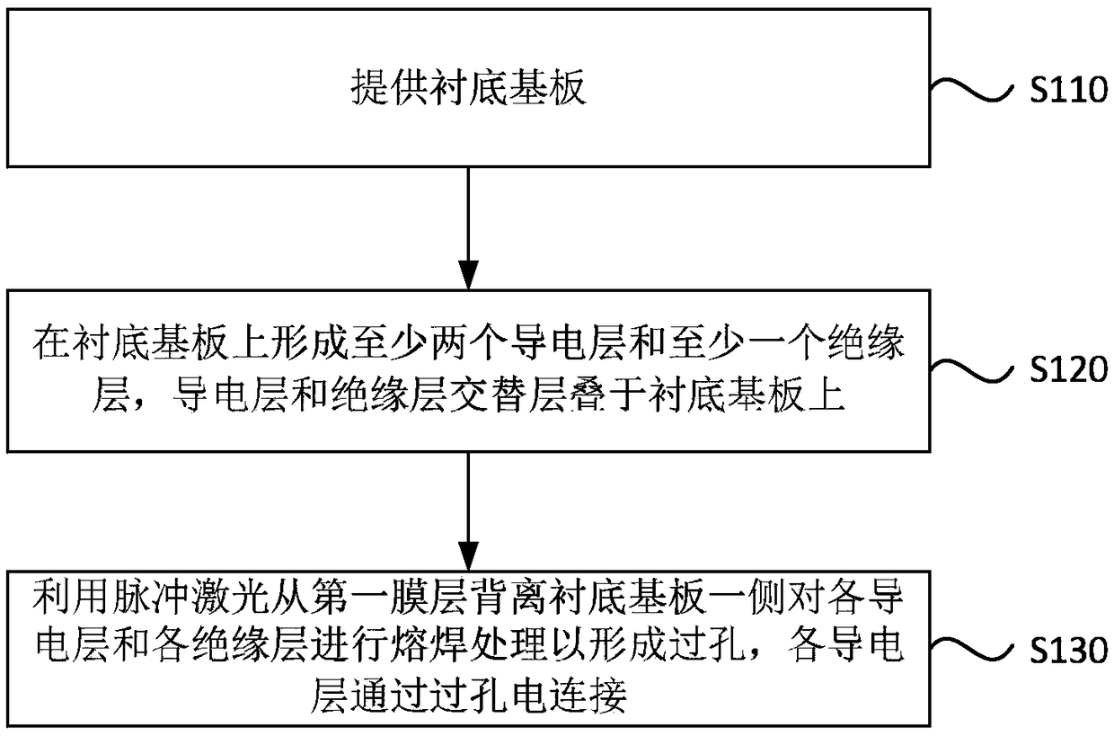
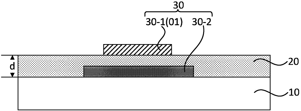
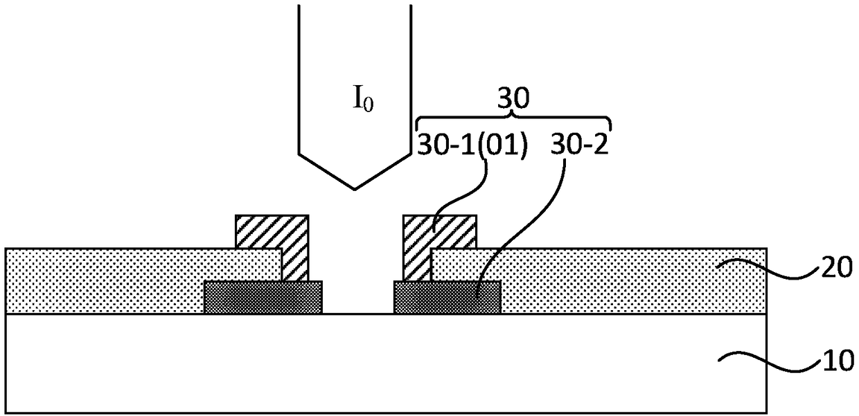
[0036] figure 1 It is a flow chart of a via hole manufacturing method provided by Embodiment 1 of the present invention. Figure 2-Figure 3 It is a schematic diagram of the structure of a conductor device in the process of forming a via hole by using a via hole manufacturing method provided in Embodiment 1 of the present invention. Combine below figure 1 and figure 2 , the manufacturing method of the via hole will be described in detail.

[0037] see figure 1 , the manufacturing method of the via includes:

[0038] S110, providing a base substrate.

[0039] see figure 2 , providing a base substrate 10 .

[0040] S120, forming at least two conductive layers and at least one insulating layer on the base substrate, where the conductive layers and the insulating layers are alternately stacked on the base substrate.

[0041] see figure 2 , at least two conductive layers 30 and at least one insulating layer 20 are formed on the base substrate 10 , and the conductive laye...

Embodiment 2

[0053] Figure 5 It is a flow chart of a via hole manufacturing method provided by Embodiment 2 of the present invention. Figure 6 It is a schematic structural diagram of a semiconductor device in the process of forming a via hole by using a via hole manufacturing method provided in Embodiment 2 of the present invention. Compared with Embodiment 1, this embodiment optimizes S130 to provide a mask plate, the mask plate includes at least one light-transmitting region and a non-light-transmitting region surrounding the light-transmitting region; place the mask plate on the first film layer The side away from the base substrate; using a pulsed laser to weld each conductive layer and each insulating layer from the side of the mask away from the first film layer to form via holes, and each conductive layer is electrically connected through the via holes.

[0054] Specifically, see Figure 5 and Figure 6 , the manufacturing method of the via includes:

[0055] S110, providing a...

Embodiment 3

[0065] Embodiment 3 of the present invention also provides a method for manufacturing an array substrate, and the method for manufacturing the array substrate includes the method for manufacturing via holes provided in any embodiment of the present invention.

[0066] In the manufacturing method of the array substrate provided by the embodiment of the present invention, each conductive layer and each insulating layer are welded from the side of the first film layer away from the base substrate by using a pulsed laser to form via holes, and each conductive layer passes through the via holes The electrical connection can replace the yellow light process. Only one welding process is required to realize the electrical connection of multiple conductive layers, which solves the problem of when multiple conductive layers need to be electrically connected during the production process of the existing display panel. It is necessary to use the yellow light process to etch each insulating...


PUM


Abstract

The embodiment of the invention discloses a through-hole manufacturing method, an array substrate manufacturing method and an array substrate. The through-hole manufacturing method comprises the following steps of: providing a substrate substrate; At least two conductive layer and at least one insulating lay are formed on that substrate, and the conductive layer and the insulating layer are alternately laminate on the substrate; Wherein a film layer having a maximum distance between the at least two conductive layers and the at least one insulating layer and the substrate is a first film layer, A laser pulse is applied to each of that conductive lay and each of the insulating layers from the side of the substrate facing away from the first film lay to form holes, and each of the conductivelayers is electrically connected through the holes. The manufacturing method of the through hole provided by the invention can realize the purpose of simplifying the manufacturing process of the holes and reducing the manufacturing cost when electrically connecting a plurality of conductive layers.

Description

technical field [0001] Embodiments of the present invention relate to semiconductor manufacturing technology, and in particular, to a method for manufacturing a via hole, a method for manufacturing an array substrate, and the array substrate. Background technique [0002] With the continuous development of display technology, electronic devices with display panels (such as mobile phones, computers, televisions, and wearable devices, etc.) have become an indispensable part of people's lives. [0003] At present, the yellow light process is used in the manufacturing process of the display panel to realize the electrical connection between different conductive layers. Specifically, a first conductive layer, a first insulating layer and a second conductive layer are sequentially formed on the base substrate. In order to ensure the electrical connection between the first conductive layer and the second conductive layer, it is usually necessary to etch the first insulating layer ...

Claims


Application Information

Patent Timeline
Patent Type & Authority Applications(China)
IPC IPC(8): H01L21/768H01L27/12B23K26/21
CPCB23K26/21H01L21/76805H01L27/1214
Inventor 徐苗周雷彭俊彪王磊邹建华陶洪
Owner SOUTH CHINA UNIV OF TECH
Why Eureka
Try Eureka