Drive signal enhancement circuit

A technology for driving signals and circuits, applied to electrical components, adjusting electrical variables, instruments, etc., can solve problems such as the failure of the system to start up normally, the failure to reach the starting value of the control IC power supply voltage, etc., to achieve design margins, prevent interference, The effect of enhanced conductivity

Pending Publication Date: 2019-01-15
MORNSUN GUANGZHOU SCI & TECH
View PDF0 Cites 0 Cited by
  • Summary
  • Abstract
  • Description
  • Claims
  • Application Information

AI Technical Summary

Problems solved by technology

When the input voltage gradually increases until the PNP transistor Q1A starts to conduct, the EC path of the PNP transistor Q1A will take a part of the base current of the PNP transistor Q1B. It can be seen that as the input voltage continues to increase, the base current of the PNP transistor Q1A The stage current also increases accordingly. Before it enters the saturation state, the base stage current of the PNP transistor Q1B gradually decreases, and it is gradually turned off from the saturation state, and the emitter voltage gradually decreases, so that the back-end BOOST boost cannot be controlled. IC power supply voltage starting value, at this time, the air switch or relay is powered on, and the system cannot start normally

Method used


Image

  • Drive signal enhancement circuit
  • Drive signal enhancement circuit
  • Drive signal enhancement circuit

Examples


no. 1 example

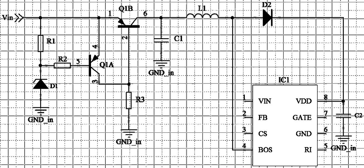
[0023] figure 2 A first example of implementation of the application of the present invention is shown.

[0024] The present invention has following 6 characteristics:

[0025] 1. The circuit is simple and the device cost is low;

[0026] 2. Isolated DC signal;

[0027] 3. With positive feedback, the driving signal is gradually enhanced;

[0028] 4. It only works when the control IC BOS pin works and the PNP transistor Q1B is turned on, and has no effect on the normal operation of the system;

[0029] 5. Not affected by device temperature characteristics and tolerances;

[0030] 6. Use an anti-reverse overvoltage diode to avoid the stress problem caused by the base level of the PNP transistor Q1B being raised during discharge, during which the PNP transistor Q1B is in a cut-off state.

[0031] A driving signal enhancement circuit, which is applied between the boost pin BOS of the control IC and the base of the triode in the low-voltage direct loop of the start-up circuit...

no. 2 example

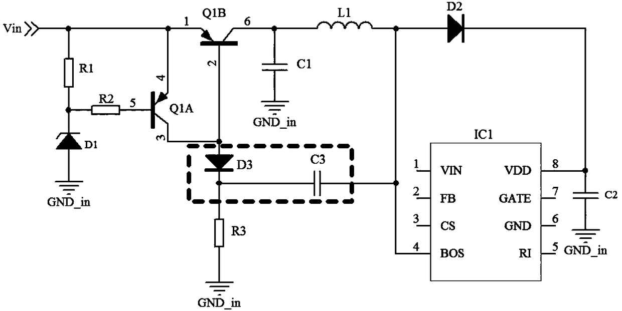
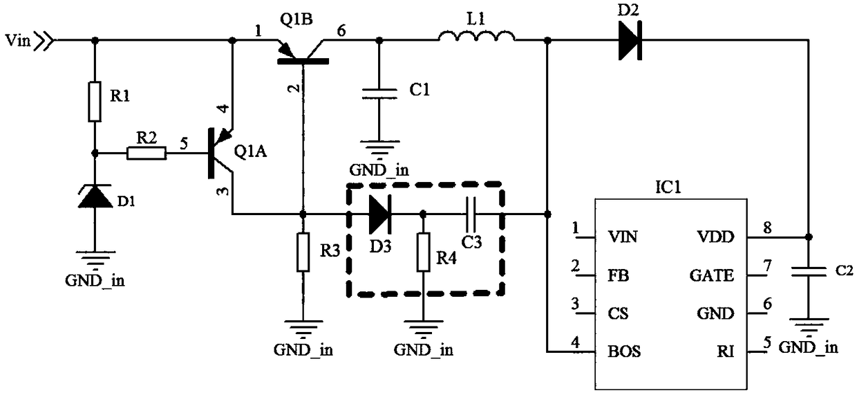
[0038] figure 2 A second example of implementation of the application of the present invention is shown.

[0039] In this embodiment, one end of the charging capacitor C3 is connected to the boost pin BOS of the control IC, and the other end is connected to the cathode of the anti-reverse overvoltage diode D3. The anode of the diode D3 is connected to the base of the PNP transistor Q1B, and the cathode of the diode D3 is connected to one end of the charging capacitor C3. One end of the bleeder resistor R4 is connected to the cathode of the diode D3, and the other end is connected to the ground.

[0040] The working principle of this embodiment is the same as the analysis of the first embodiment, here only the working principle of the bleeder circuit is described as follows:

[0041] When the internal switch of the control IC BOS pin is turned off, the capacitor C3 is discharged through the discharge resistor R4. At this time, the discharge resistor R4 also serves as a part ...


PUM


Abstract

A drive signal enhancement circuit which is applied between the boost pin BOS of the control IC and the base of the transistor in the low-voltage through loop of the startup circuit, The triode driving signal is enhanced by the charging and discharging action of the capacitor C3, so that the PNP transistor Q1B can only work in the saturated conduction (or approaching saturated conduction) or off state when the air switch or relay is started at different input voltages, so as to ensure that the voltage at the supply terminal of the control IC can reach the on value. The triode driving signal isenhanced by the charging and discharging action of the capacitor C3. The invention has the advantages of simple circuit, low realization cost and innovative avoidance of the starting dead zone of theoriginal low-voltage through loop. At that same time, the circuit of the invention only work when the pin of the control IC BOS and the PNP transistor Q1B are turned on, and has no influence on the normal steady-state operation of the system.

Description

technical field [0001] The invention relates to a drive signal enhancement circuit, in particular to a triode drive signal enhancement circuit. Background technique [0002] In a switching power supply applied to a wide-voltage input range, the startup circuit needs to meet the functions of low-voltage direct connection and high-voltage limitation at the same time, that is, it needs to be able to directly obtain power from the input voltage at low voltage to supply power to the power supply terminal of the control IC, and at high voltage, it needs to withstand the potential difference. Protect the back-end control IC from overvoltage or damage. [0003] In an ultra-wide voltage input power supply, its start-up circuit includes a high-voltage limiting circuit formed by a start-up circuit chip and a low-voltage straight-through circuit formed by two PNP transistors to meet the input range of 4.5-36VDC. The present invention only relates to the low-voltage straight-through cir...

Claims


Application Information

Patent Timeline
Patent Type & Authority Applications(China)
IPC IPC(8): H02M3/156
CPCH02M3/156
Inventor 林泽钦
Owner MORNSUN GUANGZHOU SCI & TECH
Why Eureka
Try Eureka