Through-silicon-via channel testing device

A test device and through-silicon via technology, which is applied in the field of microsystem testing, can solve the problems of cumbersome test operation steps and high manufacturing cost of the test platform, and achieve the effects of simple structure, low manufacturing cost and avoiding breakage

Pending Publication Date: 2019-01-25
THE 13TH RES INST OF CHINA ELECTRONICS TECH GRP CORP
View PDF0 Cites 2 Cited by
  • Summary
  • Abstract
  • Description
  • Claims
  • Application Information

AI Technical Summary

Problems solved by technology

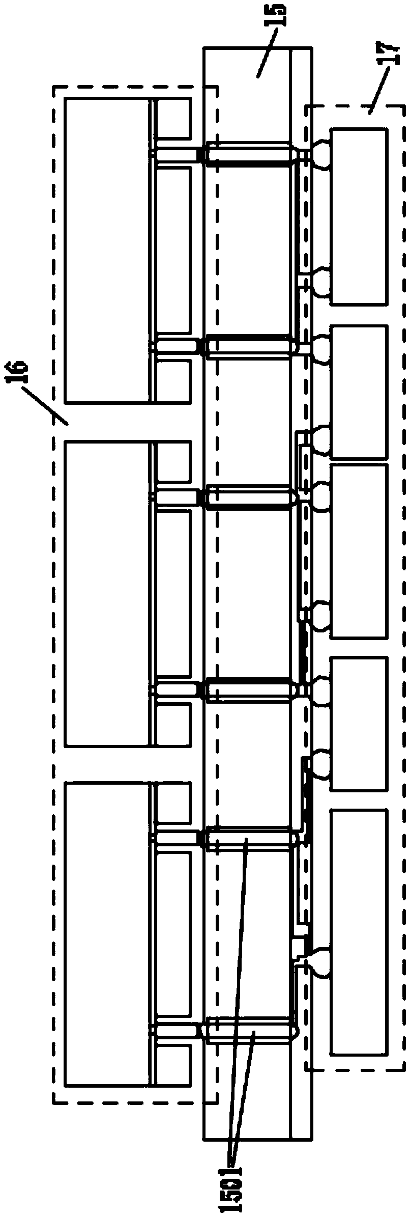
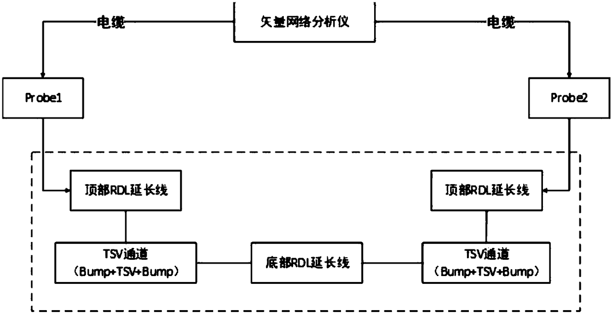
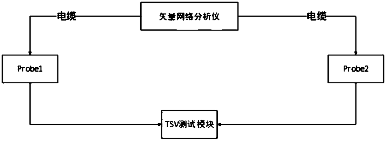
[0006] The purpose of the present invention is to provide a TSV channel testing device, which aims to solve the technical problems of high manufacturing cost of the test platform and cumbersome test operation steps existing in the prior art when testing TSV channels

Method used


Image

  • Through-silicon-via channel testing device
  • Through-silicon-via channel testing device
  • Through-silicon-via channel testing device

Examples


Embodiment Construction

[0030] In order to make the technical problems, technical solutions and beneficial effects to be solved by the present invention clearer, the present invention will be further described in detail below in conjunction with the accompanying drawings and embodiments. It should be understood that the specific embodiments described here are only used to explain the present invention, not to limit the present invention.

[0031] It should be noted that terms such as "installation", "connection", "connection", "fixation" and "setup" should be understood in a broad sense, for example, it may be a fixed connection or a Detachable connection, or integration; it can be mechanical connection or electrical connection; it can be direct connection or indirect connection through an intermediary, and it can be the internal communication of two components or the interaction relationship between two components. Those of ordinary skill in the art can understand the specific meanings of the above ...


PUM


Abstract

The invention is applicable to the technical field of micro-system tests, and provides a through-silicon-via channel testing device, which comprises a mounting base and at least one group of probe assemblies which are used for testing a through-silicon-via channel and supporting a through-silicon-via adapter plate, wherein each probe assembly comprises a first spring test probe and a second springtest probe, the mounting base comprises a first support portion and a second support portion, the first spring test probe is arranged on the first support portion, and the second spring test probe isarranged on the second support portion. The through-silicon-via channel testing device overcomes the defects that the conventional probe station testing method has high threshold, faces the through-silicon-via channel indirectly and the like through arranging the first support portion and the second support portion which can be used for testing both ends of the through-silicon-via channel simultaneously, reduces the operation steps and is simple in operation compared to the existing testing method, and has the advantages of simple structure, low manufacturing cost and easy popularization.

Description

technical field [0001] The invention belongs to the technical field of microsystem testing, and more specifically relates to a through-silicon via channel testing device. Background technique [0002] See figure 1 , Through Silicon Via (TSV, Through Silicon Via) channel, with TSV adapter board as the carrier, is the key electrical unit of vertical interconnection in 2.5D / 3D packaging structure, and TSV channel is also the third generation microsystem The core composition in packaging technology. The TSV interposer board has a rectangular or regular polygonal board (chip) structure. [0003] Compared with the previous two generations of packaging, microsystem packaging based on TSV interconnection technology enables chips to be stacked with more layers in the vertical direction. Since TSV technology greatly reduces the area occupied by gold wires and pads, the ratio of chip area to package area is close to the limit. In addition, TSV technology has better compatibility wi...

Claims


Application Information

Patent Timeline
Patent Type & Authority Applications(China)
IPC IPC(8): G01R1/067G01R1/073
CPCG01R1/06722G01R1/073
Inventor 冉红雷黄杰彭浩盛晓杰
Owner THE 13TH RES INST OF CHINA ELECTRONICS TECH GRP CORP
Why Eureka
Try Eureka