
A visible light band silicon nitride beam deflection chip

A technology of beam deflection and silicon nitride, which is applied in light guides, optics, optical components, etc., can solve the problem of low transmission loss and achieve the effect of wide bandwidth, large manufacturing tolerance, and uniform beam splitting

Active Publication Date: 2020-04-07
UNIV OF SHANGHAI FOR SCI & TECH
View PDF6 Cites 0 Cited by
  • Summary
  • Abstract
  • Description
  • Claims
  • Application Information

AI Technical Summary

Problems solved by technology

Although silicon nitride beam deflection chips in the visible light band have low transmission loss, simple structure, good optical performance, and are easy to integrate into photonic integrated circuits, there are no reports on silicon nitride beam deflection chips in the visible light band.

Method used


Image

  • A visible light band silicon nitride beam deflection chip
  • A visible light band silicon nitride beam deflection chip
  • A visible light band silicon nitride beam deflection chip

Examples


Embodiment Construction

[0029] The silicon nitride beam deflection chip in the visible light band of the present invention will be described in more detail below in conjunction with schematic diagrams, wherein a preferred embodiment of the present invention is shown, and it should be understood that those skilled in the art can modify the present invention described here and still implement the present invention. Beneficial effects of the invention. Therefore, the following description should be understood as the broad knowledge of those skilled in the art, but not as a limitation of the present invention.

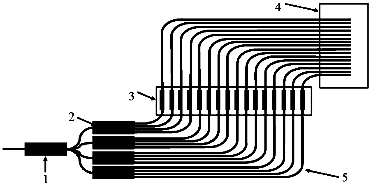
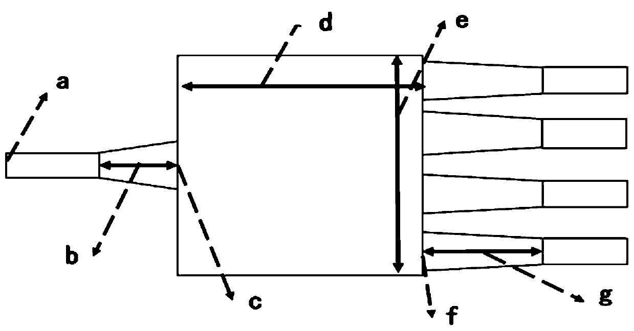
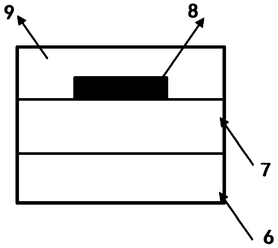
[0030] Such as figure 1 As shown, a silicon nitride beam deflection chip in the visible light band includes a silicon-based substrate 6, a silicon dioxide buffer layer 7, a silicon dioxide cladding layer 9 and a core layer 8 based on a silicon nitride waveguide; the silicon dioxide buffer layer 7 is arranged on the silicon-based substrate 6; the silicon dioxide cladding layer 9 is attached on th...


PUM

PropertyMeasurementUnit
lengthaaaaaaaaaa
lengthaaaaaaaaaa
widthaaaaaaaaaa

Abstract

The present invention provides a visible light band silicon nitride beam deflection chip. The chip comprises a silicon based substrate, a silicon dioxide buffer layer, a silicon dioxide cladding layerand a silicon nitride waveguide-based core layer; the silicon dioxide buffer layer is disposed on the silicon base substrate; the silicon dioxide cladding layer is attached to the silicon dioxide buffer layer; the core layer comprises a light beam splitting unit, a first curved waveguide, a second curved waveguide, a thermo-optical phase shifter, and an outgoing waveguide array; the light beam splitting unit, the first curved waveguide, the second curved waveguide and the outgoing waveguide array are arranged in the silicon dioxide cladding layer and are located on the silicon dioxide bufferlayer; the thermo-optical phase shifter is arranged on the silicon dioxide cladding layer; the light beam splitting unit includes a plurality of silicon nitride waveguide-based beam splitters; and theworking bandwidth of the beam splitters ranges from 480 nm to 645 nm. The chip of the invention is based on silicon nitride. The chip has the advantages of small size, compact structure and simple processing, large manufacturing tolerance, high product yield, and capability of realizing uniform beam splitting, phase modulation and beam deflection of visible light.

Description

technical field [0001] The invention belongs to the technical field of integrated photonic chips, in particular to a silicon nitride light beam deflection chip in the visible light band. Background technique [0002] In recent years, silicon-based photonics has attracted great attention from academia and industry, and has great application prospects in the fields of integrated optical communication devices, on-chip optical interconnection, biophotonics, and nonlinear optics, and is developing rapidly. A large number of infrared light beam deflection chips made of silicon materials are widely used in lidar systems and optical communication systems, and exhibit low loss, high precision, and fast scanning. Silicon-based optoelectronic technology is the use of complementary metal oxide semiconductor (CMOS) technology to realize the integrated preparation of photonic devices. This technology combines the advantages of CMOS technology's ultra-large-scale logic, ultra-high-precisio...

Claims


Application Information

Patent Timeline
Patent Type & Authority Patents(China)
IPC IPC(8): G02B6/125G02B6/126
CPCG02B6/125G02B6/126G02B2006/12061
Inventor 冯吉军仲路铭张福领曾和平
Owner UNIV OF SHANGHAI FOR SCI & TECH
Learn More