
Silicon nitride phased array chip based on suspended waveguide structure

A technology of suspended waveguide and silicon nitride, which is applied in the direction of optical waveguide light guide, light guide, instrument, etc., can solve the problem of the difference in refractive index between the silicon nitride core layer and the silicon oxide cladding layer, the coupling crosstalk between the waveguides, and the far-field outgoing beam Quality deterioration and other problems, to achieve the effect of large production tolerance, compact structure and simple processing

Active Publication Date: 2020-12-04
华东师范大学重庆研究院 +6
View PDF0 Cites 0 Cited by
  • Summary
  • Abstract
  • Description
  • Claims
  • Application Information

AI Technical Summary

Problems solved by technology

[0007] However, limited by the refractive index difference between the silicon nitride core layer and the silicon oxide cladding layer, the distance between waveguide elements is small, and coupling crosstalk is prone to occur between adjacent waveguides, which deteriorates the quality of the far-field outgoing beam.
Therefore, the silicon nitride phased array beam deflection chips that have been reported so far usually have a large spacing between the waveguide elements, resulting in side lobes that are closer to the main peak, which limits the beam scanning range.

Method used


Image

  • Silicon nitride phased array chip based on suspended waveguide structure
  • Silicon nitride phased array chip based on suspended waveguide structure
  • Silicon nitride phased array chip based on suspended waveguide structure

Examples


Embodiment Construction

[0034] The following examples will make a further description of the present invention in conjunction with the accompanying drawings. This example prepares a silicon nitride phased array chip based on a suspended waveguide structure, but this example cannot be used to limit the present invention. Any similar method of the present invention is adopted And similar changes thereof should be included in the protection scope of the present invention.

[0035](1) Device design

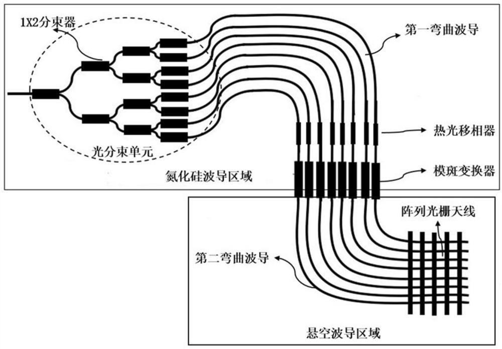
[0036] For the silicon nitride phased array chip based on the suspended waveguide structure, the present invention uses a light source with a wavelength of 1550nm to reach the designed array grating antenna through a designed silicon nitride beam splitter to realize wide field of view beam scanning.

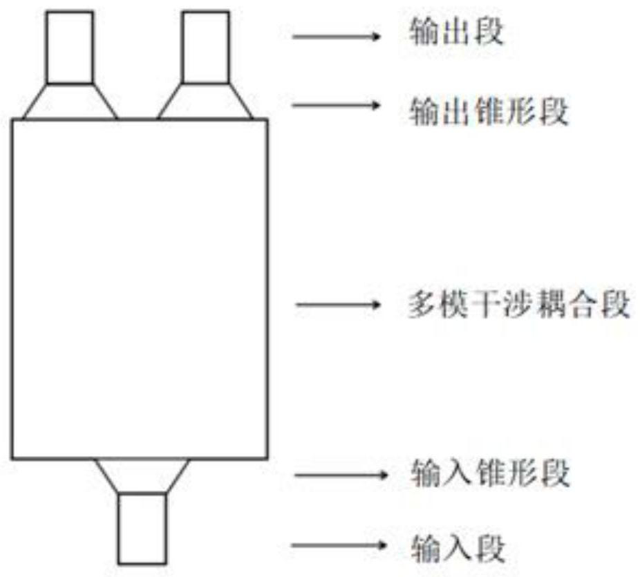
[0037] For the silicon nitride beam splitter, a straight waveguide with a width w=10 μm is selected at a wavelength of 1550 nm, and then the multimode interference length of the beam splitter is obtained throug...


PUM

PropertyMeasurementUnit
Widthaaaaaaaaaa
Lengthaaaaaaaaaa
Lengthaaaaaaaaaa

Abstract

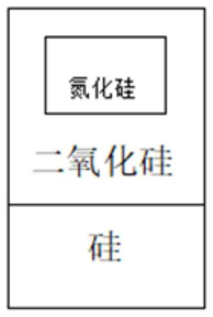
The invention discloses a silicon nitride phased array chip based on a suspended waveguide structure. The silicon nitride phased array chip comprises a silicon nitride waveguide region and a suspendedwaveguide region, wherein the silicon nitride waveguide region II is composed of a silicon-based substrate, a silicon dioxide buffer layer, a silicon dioxide cladding and a silicon nitride waveguide-based core layer; the core layer comprises a light beam splitting unit, a first bent waveguide, a thermo-optical phase shifter and a spot size converter; and the suspended waveguide region comprises asecond bent waveguide and an array grating antenna. The silicon nitride phased array chip based on a suspended waveguide structure has a good application prospect in video imaging, bioluminescence detection, and optical phased array light beam deflection and scanning.

Description

technical field [0001] The invention belongs to the technical field of integrated photonic chips, and in particular relates to a silicon nitride phased array chip based on a suspended waveguide structure in the 1550nm band. Background technique [0002] With the rapid development of silicon-based optoelectronic integration technology, silicon-based photonics technology has been widely studied, and thousands of optoelectronic devices can be integrated on a chip. This technology is suitable for making laser radar light emitting modules, called optical phased array. A large number of infrared beam scanning chips made of silicon materials are widely used in lidar systems and optical communication systems, and exhibit low loss, high precision, high stability, anti-interference, small size and fast scanning. . Silicon-based optoelectronics technology is the use of complementary metal oxide semiconductor (CMOS) technology to realize the integrated preparation of photonic devices....

Claims


Application Information

Patent Timeline
IPC IPC(8): G02B6/124G02B6/12G02B6/122G02B6/125
CPCG02B6/124G02B6/125G02B6/12009G02B6/1228G02B2006/12107G02F1/0147G02B6/12014G02B6/12016G02B2006/12061G02B2006/1215
Inventor 曾和平冯吉军胡梦云李小军谭庆贵葛锦蔓
Owner 华东师范大学重庆研究院
Learn More