A TSV hole filling method
A technology of aperture and blind hole, applied in electrical components, semiconductor/solid-state device manufacturing, circuits, etc., can solve problems such as poor effect, low filling rate, and excessively thick surface Cu layer, to simplify operation complexity and reduce processing. Effects of difficulty, good orifice condition
- Summary
- Abstract
- Description
- Claims
- Application Information
AI Technical Summary
Problems solved by technology
Method used
Image
Examples
Embodiment Construction
[0044] Hereinafter, the present invention will be further described in conjunction with the drawings and specific embodiments.
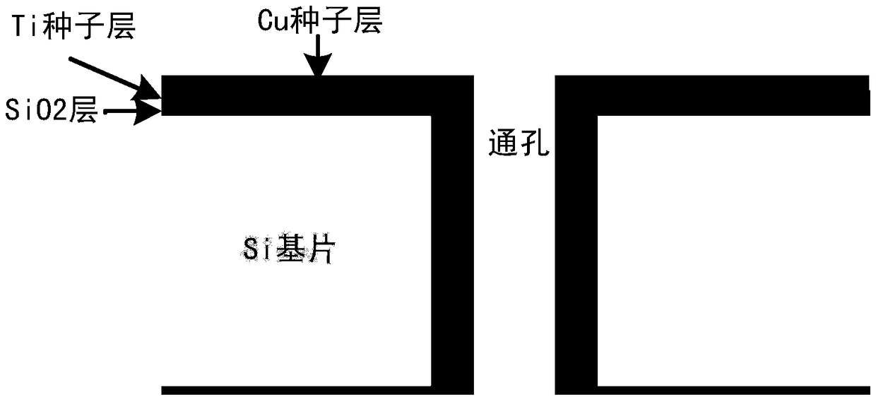
[0045] Such as Figure 1 to 4 As shown, a TSV hole filling method specifically includes the following steps:
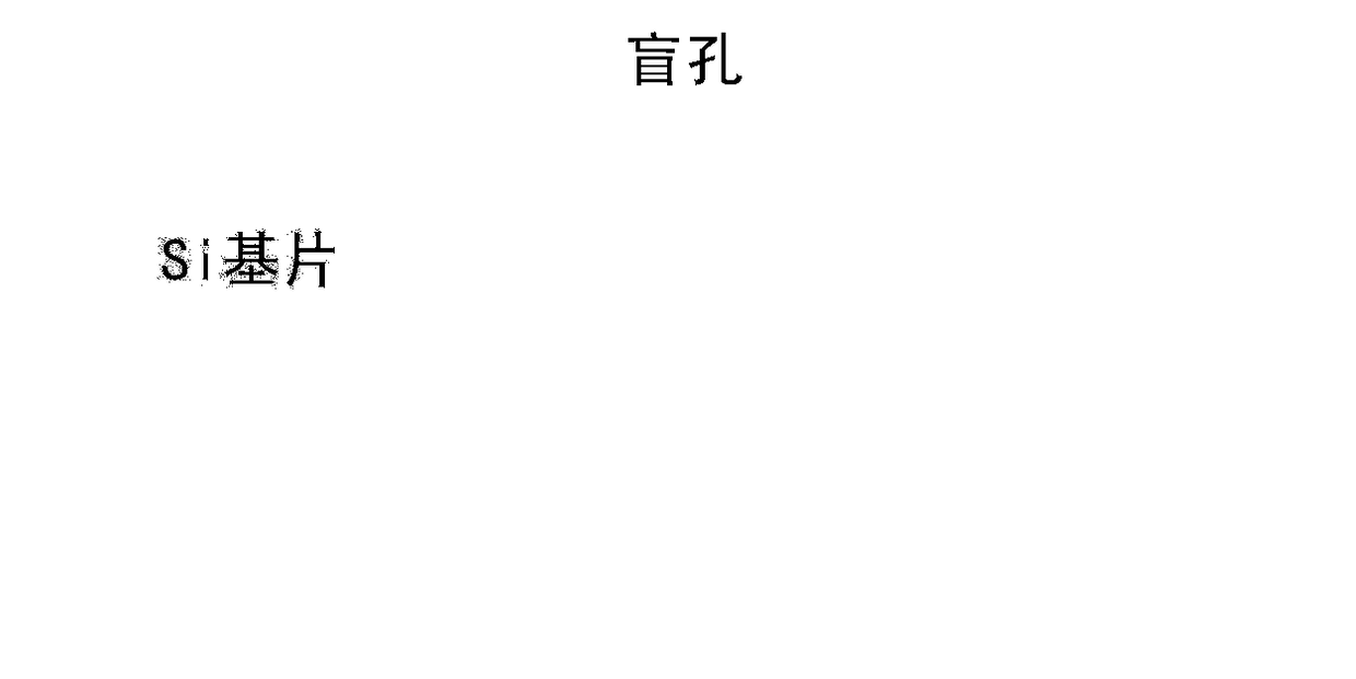
[0046] (1) Perform photolithography and etching on the front surface of the Si substrate to obtain blind holes with a diameter of 5 to 150 μm and a depth of 100 to 350 μm, and then remove the glue. The processed structure is as follows figure 1 Shown
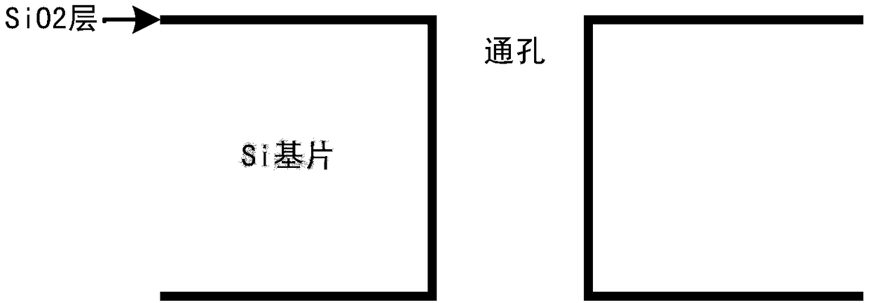
[0047] (2) Grind and polish the back of the substrate treated in step (1) until the etching holes are exposed, clean, dry, and grow SiO on both sides 2 Layer, the processed structure is like figure 2 Shown
[0048] (3) The substrate processed in step (2) is subjected to backside filming treatment;
[0049] When the substrate is subjected to back filming treatment, a filming machine is used to paste UV film, blue film, etc. on the back of the silicon wafer, and the excess film is cut along the edge of ...
PUM
 Abstract
Description
Claims
Application Information


