micropore manufacturing method and a structure of a PCB substrate

A manufacturing method and microporous technology, applied in printed circuit manufacturing, electrical connection printed components, electrical components, etc., can solve the problems of high R&D and production costs, reduced volume, and no equipment, so as to increase circuit density and reduce hole size , Improve the effect of circuit integration

Pending Publication Date: 2019-01-25
深圳和美精艺半导体科技股份有限公司
View PDF0 Cites 1 Cited by
  • Summary
  • Abstract
  • Description
  • Claims
  • Application Information

AI Technical Summary

Problems solved by technology

[0002] As we all know, with the development of electronic circuit technology, it is necessary to make more dense circuit layers on the PCB substrate of the same size to improve the integration of products and reduce the volume. In the current field of packaging PCB substrates, PCB substrates are developed. Holes are mainly opened by laser, and the minimum diameter of blind holes opened by laser is 50um. If you need to make holes smaller than 50um, such as 30um holes, you need to use special equipment, and the development and production costs of such equipment are extremely high. And there is currently no related equipment that can be purchased
However, if the hole size cannot be broken through, it is impossible to produce ultra-high-density wiring packaging substrates, which is the main shortcoming of traditional technologies.

Method used


Image

  • micropore manufacturing method and a structure of a PCB substrate
  • micropore manufacturing method and a structure of a PCB substrate

Examples


Embodiment Construction

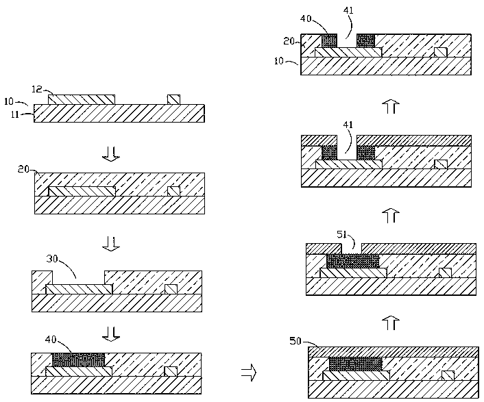
[0018] Such as Figures 1 to 2 As shown, a method for manufacturing microholes on a PCB substrate includes the following steps.

[0019] The first step is to manufacture the circuit board 10 .

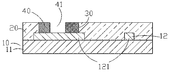
[0020] The circuit board 10 includes a substrate layer 11 and a copper-clad circuit layer 12, the copper-clad circuit layer 12 is arranged on the top surface of the substrate layer 11, and the copper-clad circuit layer 12 is pressed on the substrate layer 11 top surface The circuit board 10 is formed on the substrate, the copper-clad circuit layer 12 is processed into a predetermined circuit pattern, and the substrate layer 11 includes a glass fiber layer and an epoxy resin layer.

[0021] In practice, the circuit board layer 10 is formed by laminating the glass fiber layer, the epoxy resin layer and the copper-clad circuit layer 12. The circuit board layer 10 has relevant requirements on the TG value, which is the so-called FR-4 , the TG of general epoxy resin is 120-130°C, and the ...


PUM


Abstract

The invention relates to a micropore manufacturing method of a PCB substrate and a structure thereof, The method comprises the steps of, the first step is to make the circuit board, Step 2, baking thecircuit board in the first step; step 3, covering the dielectric layer on the top surface of the circuit board; step 4, opening a blind hole on the dielectric layer; step 5, setting a dielectric material block; step 6, setting a photoresist layer; step 7, opening a window hole in the photoresist layer; step 8, processing a microhole; and step 9, removing the photoresist layer to obtain a finishedproduct.

Description

technical field [0001] The invention relates to a method for opening holes in a PCB substrate and a hole structure thereof, in particular to a method capable of reducing the size of holes in a PCB substrate and a structure thereof. Background technique [0002] As we all know, with the development of electronic circuit technology, it is necessary to make more dense circuit layers on the PCB substrate of the same size to improve the integration of products and reduce the volume. In the current field of packaging PCB substrates, PCB substrates are developed. Holes are mainly opened by laser, and the minimum diameter of blind holes opened by laser is 50um. If you need to make holes smaller than 50um, such as 30um holes, you need to use special equipment, and the development and production costs of such equipment are extremely high. And there is no relevant equipment to be purchased at present. However, if a breakthrough cannot be made in the size of the opening, it is impossib...

Claims


Application Information

Patent Timeline
Patent Type & Authority Applications(China)
IPC IPC(8): H05K3/00H05K1/11
CPCH05K3/0026H05K1/115H05K3/0023
Inventor 徐亜川
Owner 深圳和美精艺半导体科技股份有限公司
Why Eureka
Try Eureka