System for chemical and/or electrolytic surface treatment

A surface treatment, chemical technology, applied in the field of systems for chemical and/or electrolytic surface treatment, capable of solving problems such as suboptimal pre-wetting methods and achieving uniform material deposition

Pending Publication Date: 2019-02-05
SEMSYSCO GMBH
View PDF3 Cites 0 Cited by
  • Summary
  • Abstract
  • Description
  • Claims
  • Application Information

AI Technical Summary

Problems solved by technology

[0009] However, this pre-wetting method is not optimal

Method used


Image

  • System for chemical and/or electrolytic surface treatment
  • System for chemical and/or electrolytic surface treatment
  • System for chemical and/or electrolytic surface treatment

Examples


Embodiment Construction

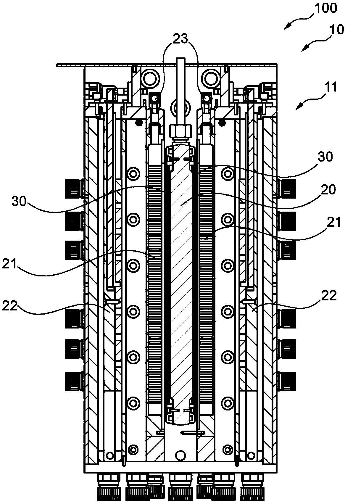
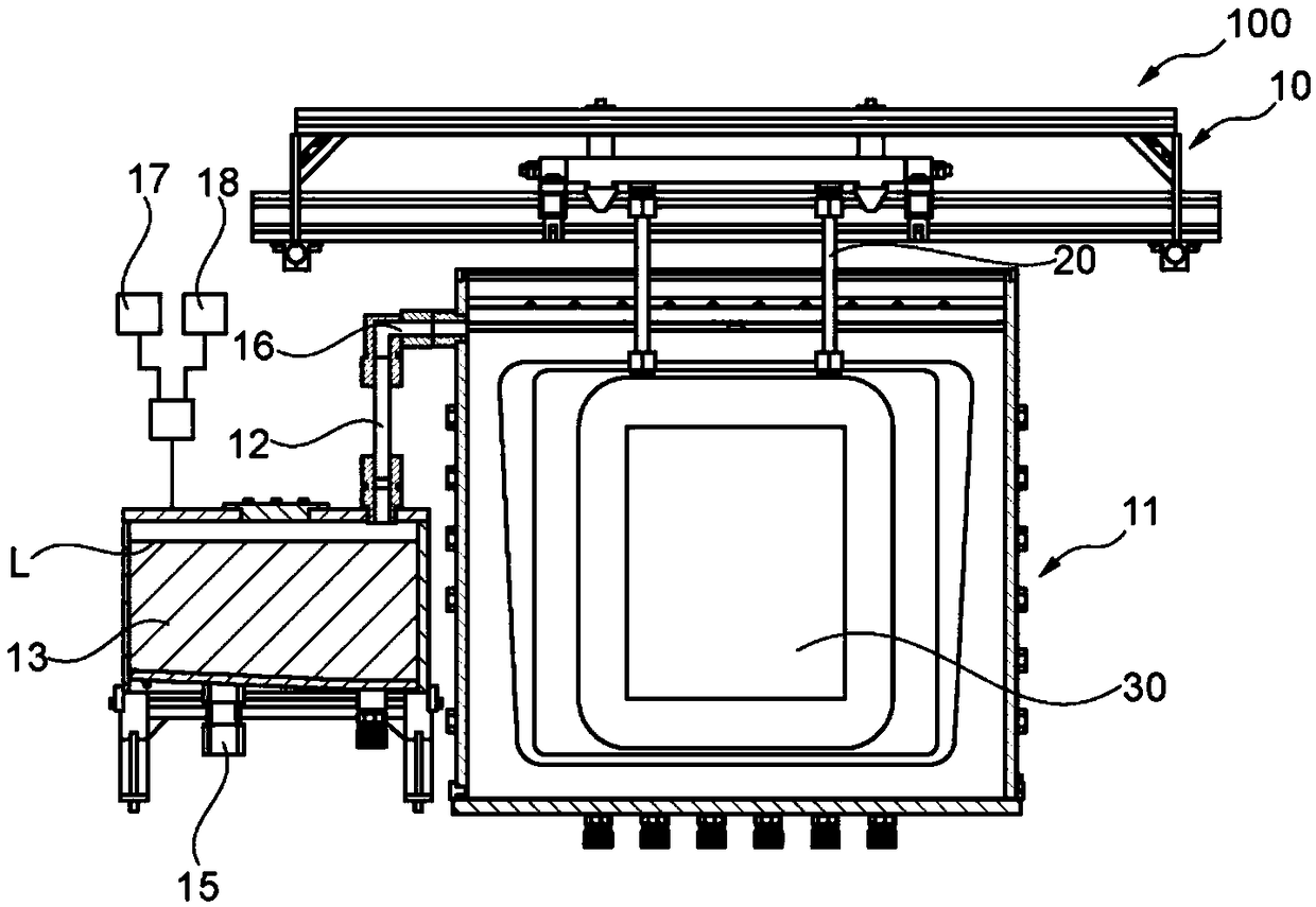
[0053] figure 1 , image 3 and Figure 4 An embodiment of a device 100 according to the invention for chemical and / or electrolytic surface treatment of a substrate 30 in a process fluid is shown schematically and exemplarily. The apparatus 100 for chemical and / or electrolytic surface treatment comprises a substrate holder 20 and a system 10 for chemical and / or electrolytic surface treatment of a substrate 30 in a process fluid.

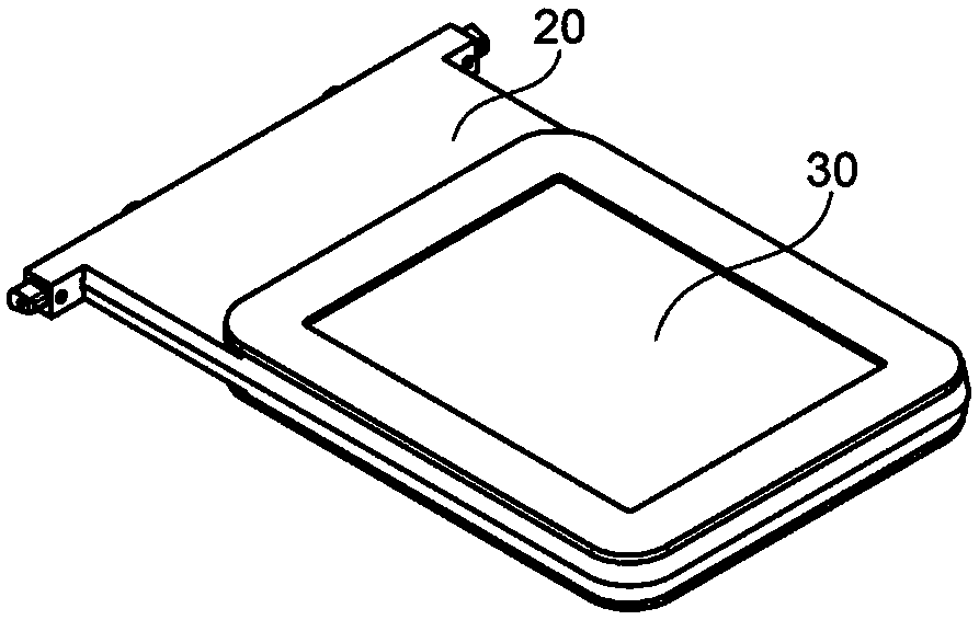
[0054] The substrate holder 20 is in figure 2 shown in and configured to hold a substrate 30 . The substrate holder 20 here holds two substrates, one substrate 30 on each side of the substrate holder 20 . The substrate holder 20 may also be configured to hold only one substrate, which may be processed from one or both sides.

[0055] Such as figure 1 , image 3 and Figure 4 The illustrated system 10 for chemical and / or electrolytic surface treatment of a substrate 30 in a process fluid produces a target flow and current density pattern for t...


PUM


Abstract

A system for chemical and / or electrolytic surface treatment of a substrate in a process fluid, a device for chemical and / or electrolytic surface treatment of a substrate in a process fluid, and a method for chemical and / or electrolytic surface treatment of a substrate in a process fluid are all described. The system for surface treatment comprises a basin, a fluid passage, an expansion tank, and acontrol unit. The basin is configured for the surface treatment of the substrate in the process fluid. The fluid passage links the basin and the expansion tank. The expansion tank is configured to hold an expansion volume of the process fluid. The control unit and the fluid passage are configured to maintain a level of the process fluid in the basin at an essentially constant level.

Description

technical field [0001] The invention relates to a system for the chemical and / or electrolytic surface treatment of a substrate in a process fluid, a device for the chemical and / or electrolytic surface treatment of a substrate in a process fluid, and a system for the chemical and / or electrolytic surface treatment of a substrate in a process fluid Methods of chemical and / or electrolytic surface treatment in process fluids Background technique [0002] In the semiconductor industry, various processes may be used to deposit material on or remove material from the surface of a wafer. [0003] For example, an electrochemical deposition (ECD) or electrochemical mechanical deposition (ECMD) process may be used to deposit conductors such as copper on a previously patterned wafer surface to fabricate device interconnect structures. [0004] Chemical mechanical polishing (CMP) is commonly used for the material removal step. Another technique, electropolishing or electroetching, can a...

Claims


Application Information

Patent Timeline
IPC IPC(8): C23C18/00C25D17/00C25D21/12C23F1/08C25F7/00C25D11/02H01L21/67
CPCC23C18/00C23F1/08C25D11/005C25D11/02C25D17/00C25D21/12C25F7/00H01L21/67017C25D17/001C25D17/02C25D21/14C25D7/12C25D21/16
Inventor 安德烈亚斯·格莱斯纳奥利佛·克诺尔托马斯·维恩斯贝格尔赫伯特·奥茨林格
Owner SEMSYSCO GMBH
Why Eureka
Try Eureka