Supercharge Your Innovation With Domain-Expert AI Agents!

A kind of processing method of multi-layer circuit board containing PTFE

A multi-layer circuit board and processing technology, which is applied in the direction of printed circuit, printed circuit manufacturing, electrical components, etc., can solve the problems that affect the quality of signal transmission and cannot be removed during processing, so as to improve processing efficiency and avoid interference of signal transmission , Avoid the abnormal effect of product combination

Active Publication Date: 2021-06-22
珠海杰赛科技有限公司 +1
View PDF0 Cites 0 Cited by
  • Summary
  • Abstract
  • Description
  • Claims
  • Application Information

AI Technical Summary

Problems solved by technology

[0003] Because PTFE is a thermoplastic material, it is easy to form a molten state when it is locally heated, and it adheres to the inner layer copper layer as the drill bit descends. The material is heated to form a molten glue, which adheres to the drill bit and the inner layer copper, and cannot be removed during the post-processing process, which affects the quality of signal transmission

Method used


Image

  • A kind of processing method of multi-layer circuit board containing PTFE
  • A kind of processing method of multi-layer circuit board containing PTFE
  • A kind of processing method of multi-layer circuit board containing PTFE

Examples


Embodiment 1

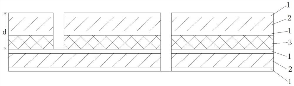
[0025] Such as figure 1 As shown, the multilayer circuit board in which the PTFE board layer and the glass cloth board layer are mixed and pressed, and the middle core board is a PTFE board layer, wherein the PTFE board layer includes PTFE, glass cloth and ceramics, and its processing method includes the following steps:

[0026] ① Cutting: Cut the copper clad laminate containing PTFE and the copper clad laminate made of glass cloth according to the design size;

[0027] ②Pattern transfer between the inner circuit board and the outer circuit board: Paste the dry film on the surface of the copper clad board, then use the inner hole of the board for alignment, expose the dry film, develop it, and etch the inner circuit board and the outer circuit board out the required graphics;

[0028] ③Lamination: Press and paste the inner circuit board and the outer circuit board to make a multi-layer circuit board, in which the core board is a PTFE board.

[0029] ④ Drilling: Drill holes ...

Embodiment 2

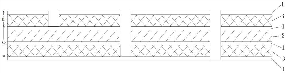
[0032] Such as figure 2 Shown, the multilayer circuit board that PTFE board layer and glass cloth board layer are mixed press, and intermediate core board is glass cloth board layer, and wherein, PTFE board layer comprises PTFE and glass cloth, and its preparation method comprises the following steps:

[0033] ① Cutting: Cut the copper clad laminate according to the design size, and the components of the two copper clad laminates include PTFE and glass cloth;

[0034] ②Pattern transfer between the inner circuit board and the outer circuit board: Paste the dry film on the surface of the copper clad board, then use the inner hole of the board for alignment, expose the dry film, develop it, and etch the inner circuit board and the outer circuit board out the required graphics;

[0035] ③Lamination: Press and paste the inner circuit board and the outer circuit board to make a multi-layer circuit board.

[0036] ④ Drilling: Drill holes on the multilayer circuit board made in ste...

Embodiment 3

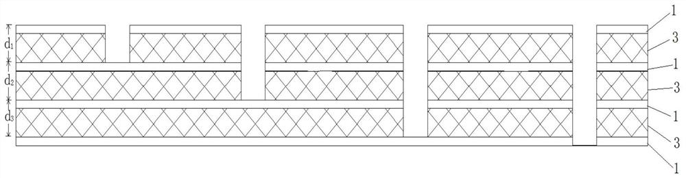
[0039] Such as image 3 Shown, the multilayer circuit board that a plurality of PTFE plate layers are mixed pressure, its preparation method comprises the following steps:

[0040] ① Cutting: Cut the copper clad laminate according to the design size, and each copper clad laminate contains PTFE and glass cloth;

[0041] ②Pattern transfer between the inner circuit board and the outer circuit board: Paste the dry film on the surface of the copper clad board, then use the inner hole of the board for alignment, expose the dry film, develop it, and etch the inner circuit board and the outer circuit board out the required graphics;

[0042] ③Lamination: Press and paste the inner circuit board and the outer circuit board to make a mixed-pressure multi-layer circuit board.

[0043] ④ Drilling: Drill holes in the multi-layer circuit board made in step ③. The drilling method adopts segmental drilling. First drill through the PTFE layer, and then drill through the remaining materials. T...


PUM


Abstract

The invention discloses a processing method for a multi-layer circuit board containing PTFE, which comprises the following steps: ① material cutting: cutting the copper clad laminate according to the designed size; Use the inner hole of the board for alignment, expose the dry film, and then develop, etch the required graphics on the inner and outer circuit boards; ③Compression: Press and paste the inner circuit board and the outer circuit board , to make a multi-layer circuit board; ④ Drilling: Drilling the multi-layer circuit board made in step ③, the drilling method adopts segmental drilling, first drill through the PTFE board layer, and then drill through the remaining materials; ⑤ Immersion copper electroplating: Carry out copper immersion electroplating on the circuit board to realize hole metallization. Using the technical solution provided by the present invention can avoid the problem of drilling contamination generated during the drilling process of the circuit board, obtain better hole wall quality, and at the same time save costs and improve work efficiency.

Description

【Technical field】 [0001] The invention relates to the technical field related to the manufacture of mixed-pressure multilayer circuit boards, in particular to a processing method for multilayer circuit boards containing PTFE. 【Background technique】 [0002] With the continuous progress and development of communication technology, more and more PCB substrates are processed with high-frequency and high-speed materials. The main material of the substrate basically belongs to the component structure of PTFE+glass fiber+ceramic, which is widely used in aerospace, aviation, etc. , satellite communications, navigation, radar and other high-tech fields. Due to the particularity of the workplace, higher reliability requirements are put forward for PCB products. PTFE is a thermoplastic material. During the machining process, it is very easy to have drilling dirt and residual PTFE glue at the interconnection position of the inner layer. At the same time, the chemical stability of PTFE...

Claims


Application Information

Patent Timeline
Patent Type & Authority Patents(China)
IPC IPC(8): H05K3/00
CPCH05K3/0047H05K2203/1476
Inventor 陈炼郑凡蒋茂胜
Owner 珠海杰赛科技有限公司
Features
  • R&D
  • Intellectual Property
  • Life Sciences
  • Materials
  • Tech Scout
  • Unparalleled Data Quality
  • Higher Quality Content
  • 60% Fewer Hallucinations
Learn More