Double-sided grinding device

A double-sided grinding, double-sided technology, applied in the direction of grinding equipment, grinding machine tools, grinding tools, etc., can solve the problems of difficulty in adequate correspondence, deterioration of flatness, and increase in the amount of travel of the outer periphery of the wafer, and achieve the effect of improving the reduction effect.

Active Publication Date: 2020-12-11
SUMCO CORP
View PDF6 Cites 0 Cited by
  • Summary
  • Abstract
  • Description
  • Claims
  • Application Information

AI Technical Summary

Problems solved by technology

[0010] However, in grinding, the outer peripheral portion of the flat plate has a larger peripheral speed relative to the wafer than the inner surface of the flat plate, so the advancing amount of the outer peripheral portion of the wafer becomes larger. Ministry of Grinding Problems
In the double-sided polishing device disclosed in the above-mentioned conventional patent document 1, the deformation of the flat plate caused by the thermal environment and the like is taken into consideration, but the difference in the circumferential speed and the amount of travel at the outer peripheral portion of the flat plate is not taken into account.
In the double-side polishing apparatus disclosed in Patent Document 1, only the polishing pressure is controlled to be uniform, so the polishing of the outer peripheral portion of the wafer proceeds quickly, and the amount of sag increases and the flatness deteriorates.
In this way, in the conventional method, in particular, the sagging of the outer peripheral portion of the wafer cannot be sufficiently suppressed, so it is difficult to polish both the flatness of the outer peripheral portion of the wafer and the flatness of the entire surface shape of the wafer, and it is difficult to sufficiently respond to recent demands.

Method used


Image

  • Double-sided grinding device
  • Double-sided grinding device
  • Double-sided grinding device

Examples


Embodiment 1

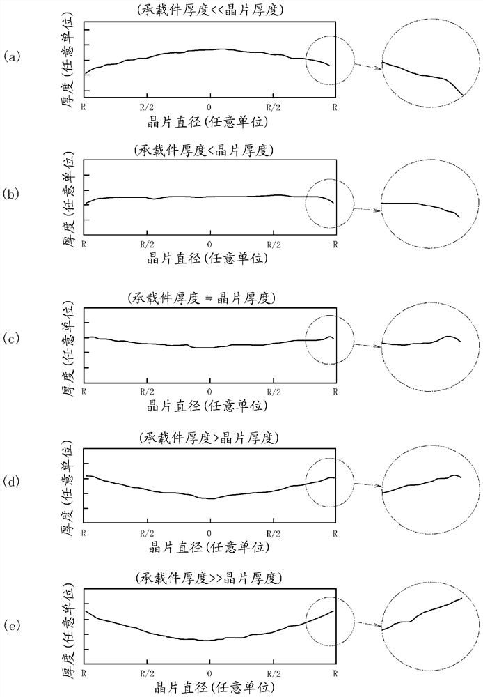
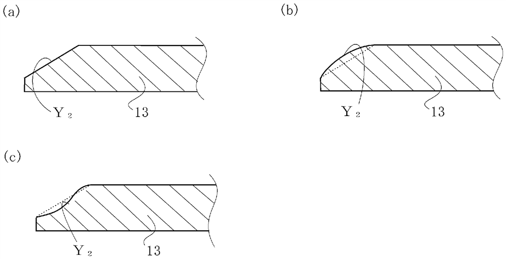
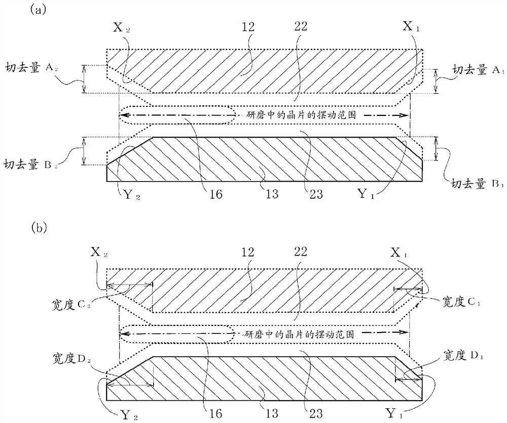
[0049] use figure 1 In the shown double-sided grinding device 10, the inner peripheral side is cut out X 1 , Y 1 The cut-off amount A in the vertical direction 1 , B 1 , Peripheral side cutting part X 2 , Y 2 The cut-off amount A in the vertical direction 2 , B 2 , Inner peripheral cutout part X 1 , Y 1 Each width of the horizontal direction C 1 、D 1 , Peripheral side cutting part X 2 , Y 2 The horizontal width C of 2 、D 2 The conditions of each test were changed as shown in Table 1 below, and both sides of the wafer were polished. Here, a silicon wafer with a diameter of 300 mm is used as the wafer. In each test case, A 1 =A 2 =B 1 =B 2 . Here, cut off part X on the inner peripheral side 1 , Y 1 Each width of the horizontal direction C 1 、D 1 , Peripheral side cutting part X 2 , Y 2 The horizontal width C of 2 、D 2 All are set to 51mm. In addition, the cut-out portion is formed by grinding each inner peripheral portion and each outer peripheral p...

Embodiment 2

[0059] use figure 1 In the shown double-sided grinding device 10, the inner peripheral side is cut out X 1 , Y 1 The horizontal width C of 1 、D 1 , Peripheral side cutting part X 2 , Y 2 The horizontal width C of 2 、D 2 The conditions of each test were changed, for example, as shown in Table 2 below, and both sides of the wafer were polished. Here, a silicon wafer with a diameter of 300 mm was used as the wafer. In addition, the coefficient α shown in Table 2 is the length of the cut-off portion with respect to the wafer diameter R, that is, by C 1 、C 2 、D 1 、D 2 =α×R represents the coefficient α. In addition, in each test example this time, C 1 =C 2 =D 1 =D 2 . In addition, the inner peripheral side cutout part X 1 , Y 1 The cut-off amount A in the vertical direction 1 , B 1 With the outer periphery side cutout part X 2 , Y 2 The cut-off amount A in the vertical direction 2 , B 2 In all Examples 1, it was fixed at 50 μm judged to be the optimum value...


PUM


Abstract

In the present invention, on each inner peripheral portion of the upper flat plate (12) and the lower flat plate (13), respectively form an inner peripheral side cutout portion ( x 1 ) and the grinding surface of the lower plate (13) slopes downward towards the inner peripheral portion of the lower plate (13). 1 ), or on each peripheral portion of the upper flat plate (12) and the lower flat plate (13), respectively form the outer peripheral side cutout portion (X 2 ) and the cut-out portion (Y 2 ), or form them all.

Description

technical field [0001] The present invention relates to a double-side polishing device which simultaneously polishes front and back surfaces of a wafer, and a double-side polishing method using the device. More specifically, it relates to a double-side polishing apparatus capable of reducing the amount of sag in the outer peripheral portion of the wafer to improve the flatness of the outer peripheral portion and the entire surface shape of the wafer, and a double-side polishing method using the same. In addition, this international application claims priority based on Japanese Patent Application No. 138464 (Japanese Patent Application No. 2016-138464) filed on July 13, 2016, and the entire content of Japanese Patent Application No. 2016-138464 is incorporated into this international application. Background technique [0002] For example, in the manufacturing process of semiconductor wafers such as silicon wafers obtained by slicing silicon single crystals, double-side polish...

Claims


Application Information

Patent Timeline
Patent Type & Authority Patents(China)
IPC IPC(8): B24B37/12B24B37/08H01L21/304
CPCB24B37/12H01L21/304B24B37/08B24B37/005B24B37/28B24B37/042B24B37/16B24B37/26B24B7/17H01L21/3043
Inventor 江崎圭佑
Owner SUMCO CORP
Why Eureka
Try Eureka