Eureka AIR delivers breakthrough ideas for toughest innovation challenges, trusted by R&D personnel around the world.

Semiconductor structure and forming method thereof

A semiconductor and mask layer technology, which is applied in the fields of semiconductor devices, semiconductor/solid-state device manufacturing, and semiconductor/solid-state device components, etc., can solve the problem of large difference in groove size, and achieve the effect of improving performance and small difference.

Inactive Publication Date: 2019-03-05
SEMICON MFG INT (SHANGHAI) CORP +1
View PDF14 Cites 10 Cited by
  • Summary
  • Abstract
  • Description
  • Claims
  • Application Information

AI Technical Summary

Problems solved by technology

[0005] However, the size of trenches formed by the sidewall quadruple patterning process in the prior art varies greatly

Method used


Image

  • Semiconductor structure and forming method thereof
  • Semiconductor structure and forming method thereof
  • Semiconductor structure and forming method thereof

Examples


Embodiment Construction

[0027] As mentioned in the background, the size of the grooves formed by the quadruple patterning process of the sidewalls is quite different.

[0028] Figure 1 to Figure 4 It is a structural schematic diagram of each step of a quadruple patterning forming method.

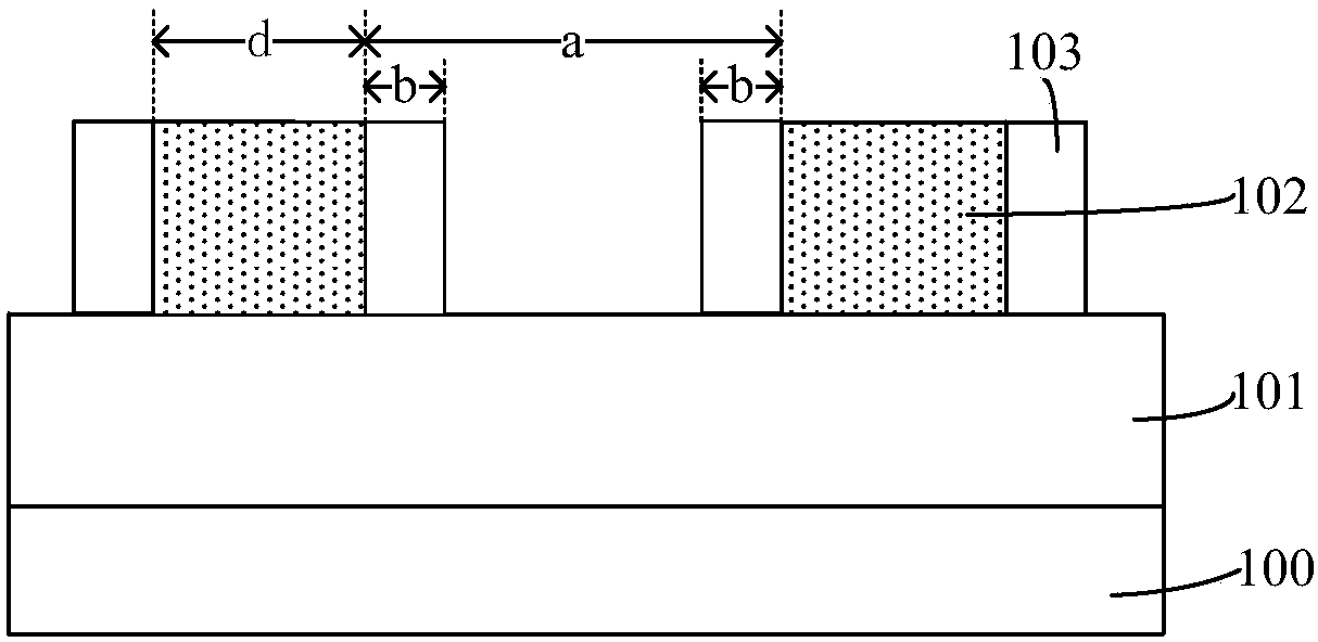
[0029] Please refer to figure 1 , providing a substrate 100, the substrate 100 has a dielectric layer 101 thereon, the dielectric layer 101 has at least one sacrificial structure 102 thereon, and the sidewall of the sacrificial structure 102 has a first sidewall 103 thereon.

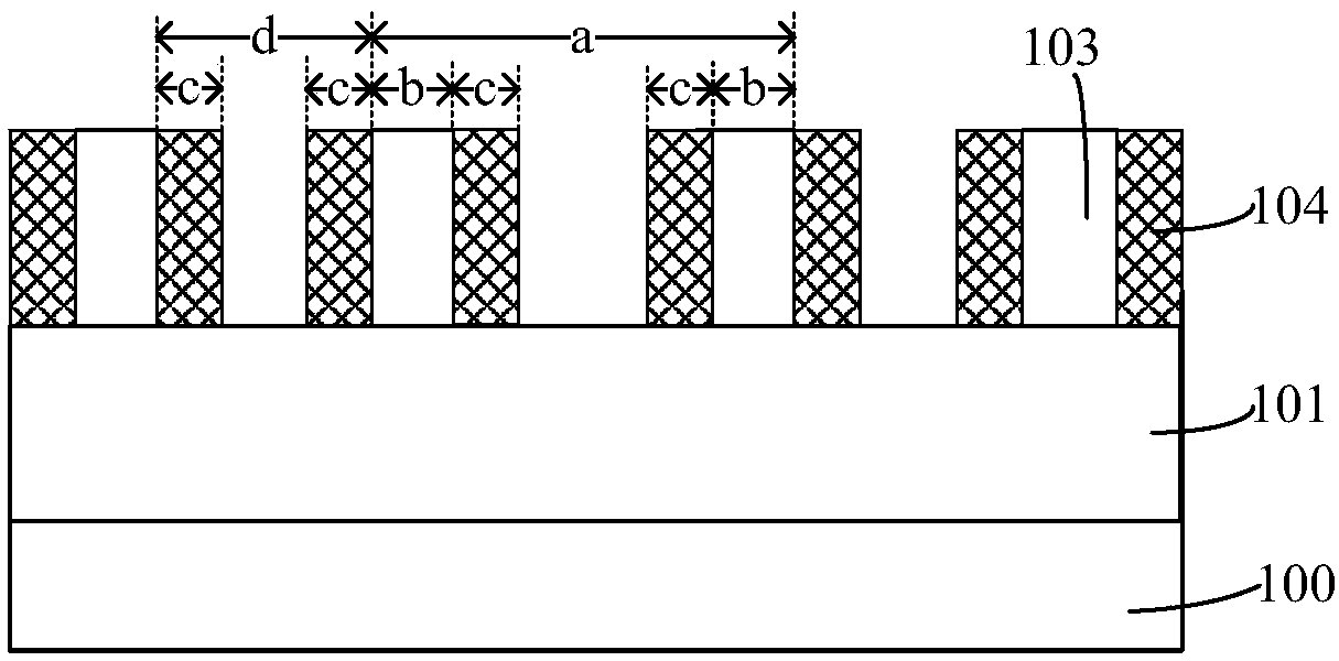
[0030] Please refer to figure 2 , after forming the first sidewall 103, removing the sacrificial structure 102 (see figure 1 ); after the sacrificial structure 102 is removed, a second sidewall 104 is formed on the sidewall of the first sidewall 103 .

[0031] Please refer to image 3 , after forming the second sidewall 104, the first sidewall 103 is removed.

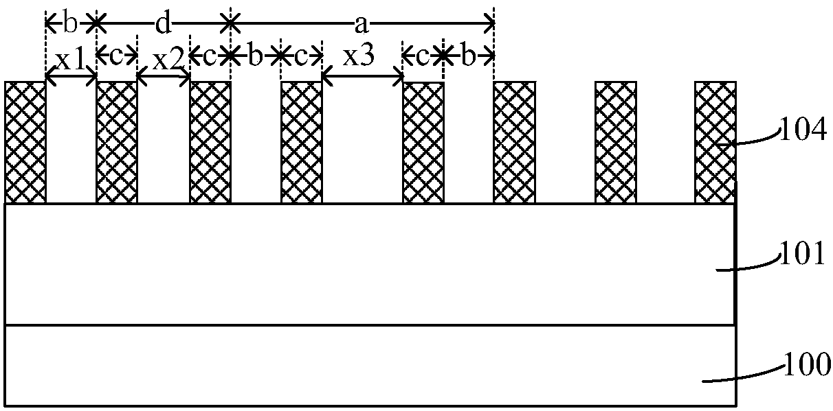
[0032] Please refer to Figure 4 After removing the first spacer 103 , t...


PUM


Abstract

The present invention discloses a semiconductor structure and forming method of the semiconductor structure, the method comprises: providing a substrate; forming a first mask layer on a portion of thesubstrate; forming a first side wall on sidewall of the first mask layer; forming a second mask layer on the substrate, wherein the second mask layer covers the sidewall of the first side wall and exposes top surface of the first side wall; after forming the second mask layer, removing the first side wall; after removing the first side wall, using the first mask layer and the second mask layer asmasks, etching a portion of the substrate to form a groove in the substrate. The method subsequently form an interconnect structures within the groove, therefore provide better performance with the interconnect structure formed by the method.

Description

technical field [0001] The invention relates to the field of semiconductor manufacturing, in particular to a semiconductor structure and a forming method thereof. Background technique [0002] In the field of semiconductor manufacturing, photoresist materials are used to transfer mask patterns to one or more material layers, for example, to transfer mask patterns to metal layers, dielectric layers or semiconductor substrates. However, as the feature size of the semiconductor process continues to shrink, it becomes more and more difficult to form a mask pattern with a small feature size in the material layer by using a photolithography process. [0003] In order to improve the integration level of semiconductor devices, various double patterning processes have been proposed in the industry, among which the self-aligned double patterning (Self-Aligned Double Patterning, SADP) process is one of them. [0004] With the further improvement of the integration of semiconductor dev...

Claims


Application Information

Patent Timeline
Patent Type & Authority Applications(China)
IPC IPC(8): H01L21/311H01L21/768H01L23/528
CPCH01L21/31144H01L21/76802H01L23/528H01L21/0337H01L21/76816H01L21/3086H01L21/3088H01L23/481H01L23/53233H01L23/53257
Inventor 陈卓凡张海洋
Owner SEMICON MFG INT (SHANGHAI) CORP
Why Eureka
Eureka Blog
Learn More