Semiconductor structure and forming method

A semiconductor and substrate technology, applied in semiconductor devices, semiconductor/solid-state device manufacturing, transistors, etc., can solve problems such as semiconductor structure performance needs to be improved, achieve the effect of improving performance, reducing the probability of residual problems, and reducing process difficulty

Active Publication Date: 2019-03-05
SEMICON MFG INT (SHANGHAI) CORP +1
View PDF5 Cites 3 Cited by
  • Summary
  • Abstract
  • Description
  • Claims
  • Application Information

AI Technical Summary

Problems solved by technology

[0004] However, the performance of semiconductor structu

Method used


Image

  • Semiconductor structure and forming method
  • Semiconductor structure and forming method
  • Semiconductor structure and forming method

Examples


Embodiment Construction

[0018] It can be seen from the background art that the performance of semiconductor devices still needs to be improved. Combining with a method of forming a semiconductor structure, the reason why its performance needs to be improved is analyzed.

[0019] refer to Figure 1 to Figure 3 , shows a structural schematic diagram corresponding to each step in a method for forming a semiconductor structure.

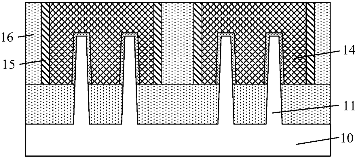
[0020] refer to figure 1 , providing a base, the base includes a substrate 10 and discrete fins 11 located on the substrate 10; a dummy gate layer 14 across the fins 11 is formed on the base, and the dummy gate layer 14 Covering part of the top and part of the sidewall of the fin 11; a sidewall 15 is formed on the sidewall of the dummy gate layer 14; an interlayer dielectric layer 16 is formed on the exposed base of the dummy gate layer 14, the The interlayer dielectric layer 16 exposes the top of the dummy gate layer 14 .

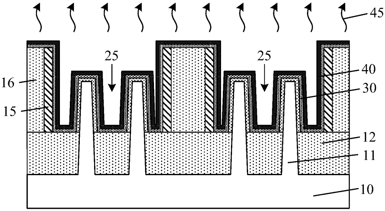
[0021] refer to figure 2 , remove the dummy gate...


PUM


Abstract

The present invention discloses a semiconductor structure and forming method of the semiconductor structure, the method comprises: providing a substrate, including a substrate and a fin on the substrate, wherein the substrate is formed with an interlayer dielectric layer, within the interlayer dielectric layer is formed with a gate opening exposing a portion of the substrate, and sidewall of the gate opening is formed a side wall; thinning a sidewall of the side wall that is away from a side of the substrate, wherein top of the side wall that is not thinned is at most flush with top of the fin; after the thinning process, forming a gate dielectric layer at bottom and the sidewall of the gate opening; forming an amorphous silicon layer on the gate dielectric layer; after the amorphous silicon layer is formed, annealing the substrate; and after the annealing process, removing the amorphous silicon layer. The method thins portion of height of the sidewall of the side wall that is away from the side of the substrate, and the top of the side wall which is not thinned is at most flush with the top of the fin, thereby reducing the probability of occurrence of an amorphous silicon layer residue problem after removal of the amorphous silicon layer.

Description

technical field [0001] The invention relates to the field of semiconductor manufacturing, in particular to a semiconductor structure and a forming method thereof. Background technique [0002] In semiconductor manufacturing, with the development trend of VLSI, the feature size of integrated circuits continues to decrease. In order to accommodate the reduction in feature size, the channel length of MOSFETs has also been shortened accordingly. However, as the channel length of the device is shortened, the distance between the source and the drain of the device is also shortened, so the ability of the gate structure to control the channel becomes worse, and the gate voltage pinches off the channel. The difficulty of the channel is also increasing, making the phenomenon of subthreshold leakage (subthreshold leakage), the so-called short-channel effect (SCE: short-channel effects) more likely to occur. [0003] Therefore, in order to better adapt to the reduction of the feature...

Claims


Application Information

Patent Timeline
IPC IPC(8): H01L21/8234H01L21/336H01L27/088
CPCH01L21/823431H01L27/0886H01L29/66795
Inventor 张焕云吴健
Owner SEMICON MFG INT (SHANGHAI) CORP
Why Eureka
Try Eureka