Packaging film and its application
A technology for encapsulating films and films, applied in semiconductor/solid-state device parts, semiconductor devices, electrical components, etc., can solve the problems of poor performance stability of electronic devices, poor water-oxygen barrier ability, and poor water-oxygen barrier properties, etc., to achieve the packaging effect. Good, enhanced water and oxygen barrier, long working life
- Summary
- Abstract
- Description
- Claims
- Application Information
AI Technical Summary
Problems solved by technology
Method used
Image

Examples
preparation example Construction
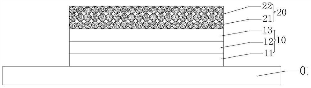
[0049] In another aspect, on the basis of the electronic device described above, an embodiment of the present invention provides a method for manufacturing the electronic device. combine Figure 1-3 , the preparation method of the electronic device includes the following steps:
[0050] providing a substrate, the substrate comprising a substrate and electronic components disposed on the substrate;
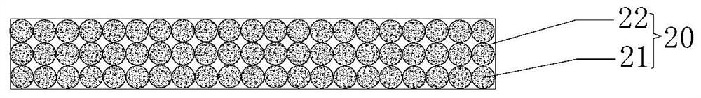
[0051] The packaging film 20 is formed on the substrate to package the electronic device.
[0052] The term "encapsulation" used in the present invention refers to covering the parts of the electronic components that need to be packaged with an encapsulation film layer. According to the realized characteristics or work requirements, different electronic component structures have different requirements for the packaged parts. Specifically, the The part where the above-mentioned electronic component needs to be packaged may be all the top surface and the side surface of the electro...
Embodiment 1
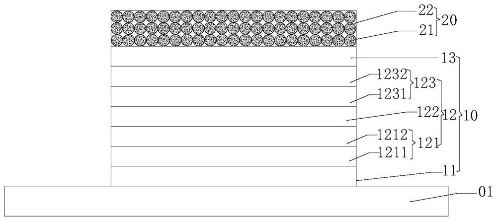
[0074] This embodiment provides an electronic device. It includes a substrate, QLED electronic components combined on the substrate and a packaging film for packaging the QLED electronic components. The structure of the electronic device is: ITO substrate / PEDOT:PSS (50nm) / poly-TPD (30nm) / quantum dot light-emitting layer (20nm) / ZnO (30nm) / silver (70nm) / encapsulation film (700nm). Wherein, the material of the packaging film is SiO 2 Ceramic grains and metal aluminum, metal aluminum filled in SiO 2 Between grains and grain boundaries, and aluminum is 1.5% of the mass of the packaging film. The thickness of the packaging film 20 is 700 nm.
[0075] The electronic device of this embodiment is prepared according to the following method:
[0076] S11: The silicon oxide nanopowder doped with aluminum metal nanoparticles is blended and ball milled by solid phase method, wherein the mass of aluminum metal nanoparticles accounts for 1.5wt% of the silicon oxide / aluminum composite mate...
Embodiment 2
[0080] This embodiment provides an electronic device. It includes a substrate, QLED electronic components combined on the substrate and a packaging film for packaging the QLED electronic components. The structure of the electronic device is: ITO substrate / PEDOT:PSS (50nm) / poly-TPD (30nm) / quantum dot light-emitting layer (20nm) / ZnO (30nm) / silver (70nm) / encapsulation film (700nm). Wherein, the material of the packaging film is to include SiO 2 Ceramic grains and metal aluminum, metal aluminum filled in SiO 2 Between grains and grain boundaries, aluminum accounts for 5% of the packaging film mass. The thickness of the packaging film 20 is 700 nm.
[0081] Its preparation method can refer to the method in the above-mentioned Example 1, only need to adjust the content of the metal in the target material to adjust, and annealing treatment is performed after the coating is completed to ensure that the low-melting point metal is doped between the ceramic grain boundaries, and the a...
PUM
| Property | Measurement | Unit |
|---|---|---|
| Melting point | aaaaa | aaaaa |
| Thickness | aaaaa | aaaaa |
| Thickness | aaaaa | aaaaa |
Abstract
Description
Claims
Application Information
 - R&D
- Intellectual Property
- Life Sciences
- Materials
- Tech Scout
- Unparalleled Data Quality
- Higher Quality Content
- 60% Fewer Hallucinations
Browse by: Latest US Patents, China's latest patents, Technical Efficacy Thesaurus, Application Domain, Technology Topic, Popular Technical Reports.
© 2025 PatSnap. All rights reserved.Legal|Privacy policy|Modern Slavery Act Transparency Statement|Sitemap|About US| Contact US: help@patsnap.com