Organic Electroluminescent Devices

An electroluminescent device and electroluminescent technology, applied in the display field, can solve problems such as low current efficiency, and achieve the effects of improving current efficiency, improving recombination area, and reducing driving voltage

Active Publication Date: 2020-05-08
KUNSHAN GO VISIONOX OPTO ELECTRONICS CO LTD
View PDF5 Cites 0 Cited by
  • Summary
  • Abstract
  • Description
  • Claims
  • Application Information

AI Technical Summary

Problems solved by technology

[0005] Therefore, the technical problem to be solved by the present invention is to overcome the defect of low current efficiency of organic electroluminescent devices in the prior art, thereby providing an organic electroluminescent device

Method used


Image

  • Organic Electroluminescent Devices
  • Organic Electroluminescent Devices
  • Organic Electroluminescent Devices

Examples


Embodiment 1

[0058] The structure of the organic electroluminescent device provided by this implementation is: ITO (20nm) / formula (I-1): F4TCNQ (4wt%, 20nm) / formula (II-1) (76nm) / AND: perylene (3wt%, 30nm) / Bphen(25nm) / Ag(16nm) / Alq3(65nm).

[0059] Wherein, ITO: indium tin oxide, is the first electrode;

[0060] AND: 9,10-bis(2-naphthyl)anthracene, a dopant material for the light-emitting layer;

[0061] Perylene: perylene, which is the main material of the light-emitting layer;

[0062] Bphen: 4,7-diphenyl-1,10-phenanthroline, an electron transport layer material;

[0063] Ag: silver, is the second electrode;

[0064] Alq3: Tris(8-hydroxyquinoline)aluminum, which is an optical coupling layer.

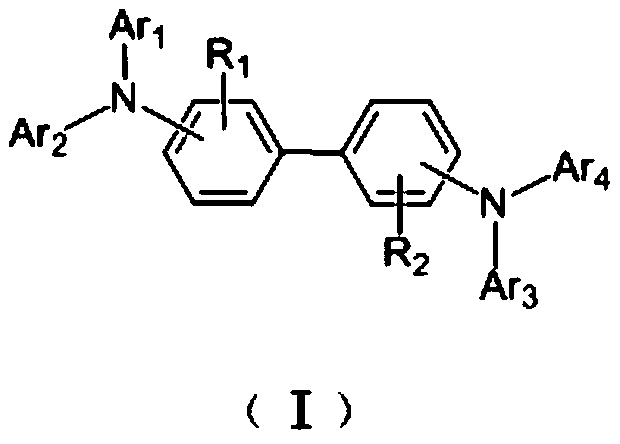
[0065] The first hole transport material is formula (I-1), the P-type dopant material is F4TCNQ, the ratio of the mass of the P-type dopant material to the mass of the first hole transport material is 4:100; the hole injection layer 30 The thickness of the hole transport layer 40 is 20 nm; the ...

Embodiment 2

[0076] This embodiment provides an organic electroluminescence device, the specific structure is the same as that of Embodiment 1, the difference is that the first hole transport material is formula (I-1), the P-type dopant material is F4TCNQ, and the hole injection layer 30 The thickness of the hole transport layer 40 is 10 nm, the doping concentration of the P-type dopant material is 8%; the second hole transport material is formula (II-2), and the thickness of the hole transport layer 40 is 86 nm.

Embodiment 3

[0078] This embodiment provides an organic electroluminescent device, the specific structure is the same as that of Embodiment 1, the difference is that the first hole transport material is formula (I-2), the P-type dopant material is F4TCNQ, and the hole injection layer 30 The thickness of the hole transport layer 40 is 10 nm, the doping concentration of the P-type dopant material is 4%; the second hole transport material is formula (II-3), and the thickness of the hole transport layer 40 is 86 nm.


PUM

PropertyMeasurementUnit
thicknessaaaaaaaaaa
thicknessaaaaaaaaaa
thicknessaaaaaaaaaa

Abstract

The present invention relates to the field of display technology, and specifically discloses an organic electroluminescent device, comprising a first electrode and a hole injection layer stacked, an ohmic contact is formed between the first electrode and the hole injection layer, and the The carrier mobility of the hole injection layer is less than 2×10 ‑5 CM 2 V ‑1 S ‑1 . The present invention reduces the mobility of holes in the organic electroluminescent device by using a material with low mobility as the hole injection layer, thereby reducing the concentration of holes in the light-emitting layer of the OLED, so that the holes in the light-emitting layer and The number of electrons tends to be balanced, which increases the recombination area of ​​holes and electrons, thereby improving the current efficiency of OLEDs.

Description

technical field [0001] The invention relates to the field of display technology, in particular to an organic electroluminescent device. Background technique [0002] Organic Light-Emitting Device (English full name Organic Light-Emitting Device, referred to as OLED) is an active light-emitting device with low power consumption, wide color gamut, and thinner volume. It is expected to become the next generation of mainstream lighting and flat panel display technology. At present, organic electroluminescent technology has been widely used in small-sized panels such as smartphone displays. [0003] Generally, an OLED includes an anode, an organic light-emitting layer, and a cathode stacked on a substrate, and a carrier functional layer interposed between the electrode and the light-emitting layer. During operation, carriers (ie, holes and electrons) are injected into the organic light-emitting layer through the anode and the cathode, and different carriers combine in the light-...

Claims


Application Information

Patent Timeline
Patent Type & Authority Patents(China)
IPC IPC(8): H01L51/54H01L51/50H01L51/52
CPCH10K85/636H10K85/633H10K50/155H10K50/17H10K50/852H10K85/631C09K11/06C09K11/08H05B33/12H10K50/00H10K50/80C07C15/04H10K85/626H10K85/6574H10K85/6576H10K50/11H10K2101/40
Inventor 闵超田景文刘胜芳
Owner KUNSHAN GO VISIONOX OPTO ELECTRONICS CO LTD
Why Eureka
Try Eureka