High-performance pucherite photo-anode film and preparation method thereof
A bismuth vanadate and photoanode technology, which is applied in chemical instruments and methods, electrodes, vanadium compounds, etc., can solve the problems of low charge mobility, slow charge separation/transport, poor oxidation kinetics, etc., and achieve high crystal quality, Good photocatalytic performance and simple method
- Summary
- Abstract
- Description
- Claims
- Application Information
AI Technical Summary
Problems solved by technology
Method used
Image
Examples
Embodiment 1
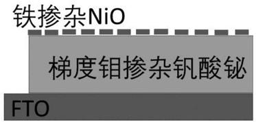
[0045] Such as figure 1 As shown, a bismuth vanadate photoanode film, the film structure includes a light absorbing layer, the upper surface of the light absorbing layer is provided with an oxygen evolution catalyst layer, the lower surface of the light absorbing layer is provided with a substrate, the The light absorbing layer is a gradient molybdenum-doped bismuth vanadate thin film, the oxygen evolution catalyst layer is an iron-doped NiO ultra-thin nanosheet, and the substrate is FTO conductive glass. The gradient molybdenum-doped bismuth vanadate thin film is doped with high concentration molybdenum on the surface. The doping concentration of the gradient molybdenum-doped bismuth vanadate thin film is 5% molar ratio.
[0046] The preparation steps of undoped bismuth vanadate thin film are as follows:
[0047] 1) Sputter a bismuth thin film on a dry, clean FTO conductive glass substrate with a length and width of 1 cm × 2 cm using a high vacuum ion sputtering apparatus; ...
Embodiment 2
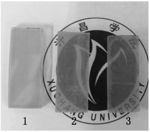
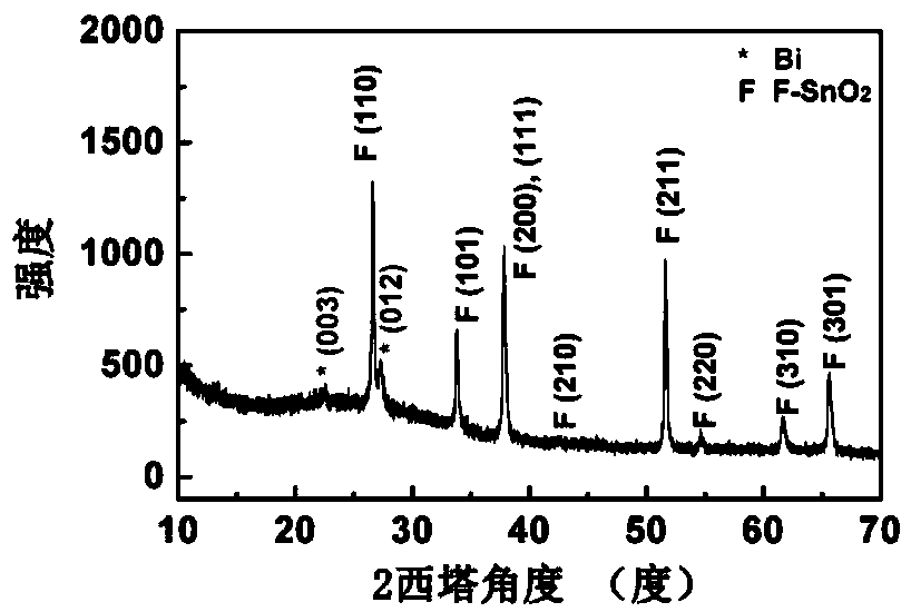
[0051] Similar to Example 1, a metal bismuth film was deposited by sputtering, and 50 microliters of vanadyl acetylacetonate and molybdenum diacetylacetonate oxide in a ratio of 19 / 1 were uniformly coated on the DMSO solution with a molar ratio of 0.5 mol / liter. , through the same drying, heat treatment, soaking, cleaning, drying and other processes as in Example 1, a uniform molybdenum-doped bismuth vanadate film was obtained. Its optical photo is attached figure 2 Medium No. 2 film. Figure 5 It is a uniform molybdenum-doped bismuth vanadate thin film, and all XRD diffraction peaks can be assigned to BiVO 4 phase with F-doped SnO 2 substrate. Figure 13 Example 2 is the performance curve of the photoanodized water prepared by this sample.
Embodiment 3
[0053] Gradient molybdenum-doped bismuth vanadate thin film preparation steps: On the undoped bismuth vanadate thin film obtained in Example 1, drop 50 microliters of vanadyl acetylacetonate and molybdenum diacetylacetonate with a ratio of 19 / 1. DMSO solution with a molar ratio of 0.5 mol / L; dried in an oven at 80-100°C and then placed in a muffle furnace at a rate of 2°C / min to first raise the temperature to 450°C and then to 500°C and keep the temperature at 500°C for 2 hours; After natural cooling, the obtained brown film is soaked in 1 mol / L NaOH solution for 20-30 minutes, washed with distilled water to remove impurity ions, and dried to obtain a gradient molybdenum-doped bismuth vanadate film. Its optical photo is attached figure 2 Medium No. 3 film.
[0054] Image 6 For gradient molybdenum-doped bismuth vanadate thin films, all XRD diffraction peaks can be attributed to BiVO 4 phase with F-doped SnO 2 substrate. Figure 7 The sample characteristic Raman signals (...
PUM
| Property | Measurement | Unit |
|---|---|---|
| thickness | aaaaa | aaaaa |
Abstract
Description
Claims
Application Information


