
Static elimination device and method for reducing static residue on surface of wafer

A static elimination device and static elimination technology, applied in the direction of static electricity, electrical components, etc., can solve the problem of residual static electricity on the wafer surface, achieve the effect of eliminating static electricity and improving product yield

Inactive Publication Date: 2019-03-08
SHANGHAI HUALI MICROELECTRONICS CORP
View PDF11 Cites 1 Cited by
  • Summary
  • Abstract
  • Description
  • Claims
  • Application Information

AI Technical Summary

Problems solved by technology

[0004] The object of the present invention is to provide a static elimination device and a method for reducing static electricity on the wafer surface, so as to solve the problem of residual static electricity on the wafer surface after the wafer in the prior art is detected by an electron scanning microscope

Method used


Image

  • Static elimination device and method for reducing static residue on surface of wafer
  • Static elimination device and method for reducing static residue on surface of wafer
  • Static elimination device and method for reducing static residue on surface of wafer

Examples


Embodiment 1

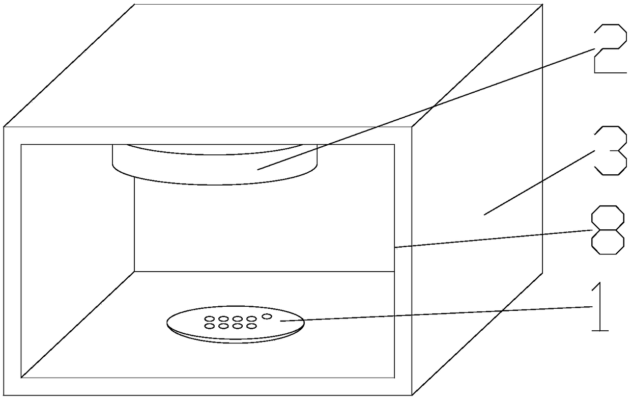
[0031] image 3 , is a schematic structural diagram of a static eliminator provided in Embodiment 1 of the present invention, please refer to image 3 . A static elimination device for eliminating static residue on the surface of a wafer 1, the static elimination device includes a static elimination unit 2 and an accommodation unit 3, and the interior of the accommodation unit 3 has a device for accommodating the wafer 1. The accommodating cavity of the circle 1, the accommodating unit 3 is provided with at least one opening 8 communicating with the accommodating cavity, the opening 8 is used to store the wafer 1, and the static elimination unit 2 is fixedly connected In the accommodating chamber, the static elimination unit 2 is used to provide ionized positive and negative ions to eliminate static electricity on the wafer 1 in a non-vacuum environment. The positive and negative charged ions formed by the ionization of the static elimination unit 2 neutralize the residual s...

Embodiment 2

[0041] Figure 7 , is a schematic structural diagram of a static eliminator provided in Embodiment 2 of the present invention, please refer to Figure 7 , the difference from Embodiment 1 is that: the number of the openings 9 is two, the accommodating unit 3 is opened along the first direction to form two through openings 9, and the static eliminator also includes a The conveyor belt 15 unit 7 for transporting the wafer 1 and the control unit for controlling the conveyor belt 15 unit 7, the conveyor belt 15 unit 7 includes a conveyor belt 15 and a motor 16, and the control unit includes a photoelectric sensor 17 and PLC controller, the conveyor belt 15 is a transparent material, the motor 16 is used to drive the conveyor belt 15 to move, and the photoelectric sensor 17 is located at the conveyor belt near the end of the journey of the conveyor belt 15 unit 7 15, the input end of the photoelectric sensor 17 is used to detect the position of the wafer 1 on the conveyor belt 15,...

Embodiment 3

[0044] The present invention also provides a method for reducing static electricity on the surface of the wafer 1, comprising the following steps: the wafer 1 passes through the above-mentioned static elimination device after being observed by the scanning electron microscope, and the positive and negative charges formed by the ionization of the static elimination unit The ions neutralize the residual static electricity on the surface of the wafer 1 to achieve the purpose of eliminating the residual static electricity on the surface of the wafer 1, and effectively prevent the residual static electricity on the surface of the wafer 1 from affecting the subsequent process, thereby improving the product yield.

[0045] In summary, the present invention provides a static elimination device and a method for reducing static electricity on the surface of a wafer. The static elimination device includes a static elimination unit and an accommodating unit, and the static elimination unit ...


PUM


Abstract

The invention provides a static elimination device and a method for reducing electrostatic residue on the surface of a wafer, for eliminating static residue on the surface of the wafer. The static elimination device comprises a static elimination unit and a receiving unit, wherein the receiving unit is internally provided with a receiving cavity for receiving the wafer and provided with at least one opening communicated with the receiving cavity; the static elimination unit is fixedly connected to the receiving cavity, and configured to perform static elimination on the wafer by providing ionized positive and negative ions in a non-vacuum environment. By neutralizing the static electricity remaining on the surface of the wafer through the positive and negative charge ions formed by ionization of the static elimination unit, the purpose of eliminating static electricity remaining on the surface of the wafer is realized, and the electrostatic residue on the surface of the wafer is effectively prevented from affecting subsequent processes, thereby improving the product yield.

Description

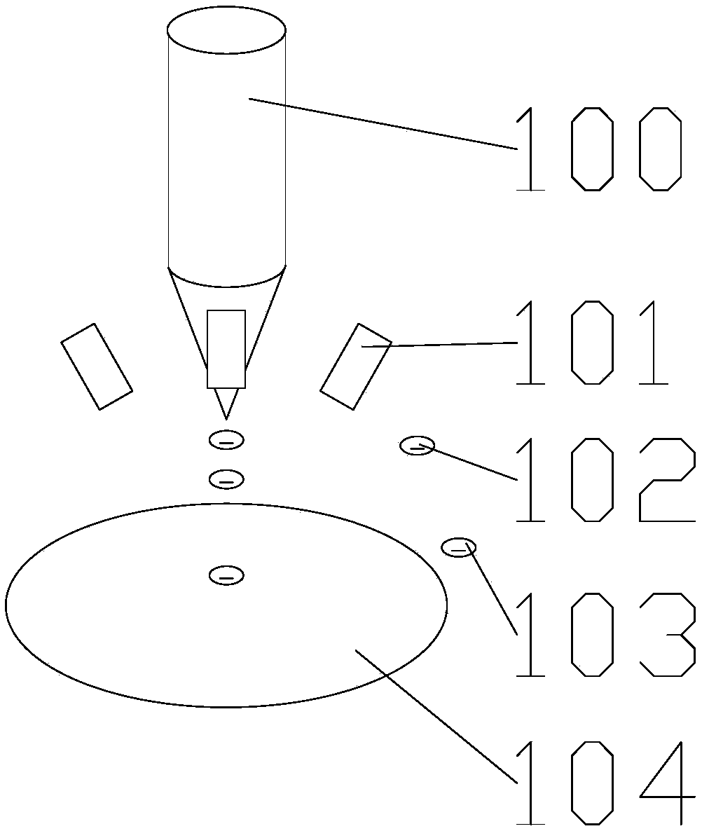
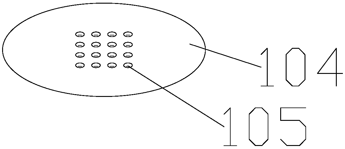
technical field [0001] The invention relates to the field of wafer manufacturing, and relates to a static elimination device and a method for reducing static residue on the wafer surface. Background technique [0002] With the development of semiconductor technology, the control of defects in the wafer manufacturing process is becoming more and more stringent, and the traditional optical defect detection can no longer fully meet the detection of defects in the wafer manufacturing process. Scanning electron microscope has become an important tool for defect analysis in the wafer manufacturing process because of its high resolution, three-dimensional image, and the ability to perform component analysis and discover electrical defects. [0003] figure 1 , is a schematic diagram of the scanning electron microscope imaging, figure 2 , is a schematic diagram of charge accumulation on the surface of a wafer 104 in the prior art, please refer to figure 1 and figure 2 , the sca...

Claims


Application Information

Patent Timeline
IPC IPC(8): H05F3/06
CPCH05F3/06
Inventor 宋箭叶
Owner SHANGHAI HUALI MICROELECTRONICS CORP
Learn More