Multi-epitaxial super-junction terminal structure and manufacturing method thereof

A technology of terminal structure and manufacturing method, applied in electrical components, circuits, semiconductor devices, etc., can solve the problems of high production cost and large area of ​​the terminal area, so as to increase the occupied area, reduce the chip area, and reduce the conduction. The effect of resistance

Pending Publication Date: 2019-03-22
WUXI NCE POWER
View PDF0 Cites 2 Cited by
  • Summary
  • Abstract
  • Description
  • Claims
  • Application Information

AI Technical Summary

Problems solved by technology

[0004] At present, a common method for preparing a superjunction structure is multiple epitaxy plus photolithography plus implantation technology, that is, first do an N-type epitaxy on the N+ type substrate material, and then photoetch the P-type silicon column area and perform P-type epitaxy. Ion implantation, followed by the second N-type epitaxy, photoetching the P-type silicon column area again and performing P-type ion implantation, and repeating the above process for the third, fourth or even more times according to the breakdown voltage requirements of the device. However, The terminal area of ​​this structure occupies a relatively large area, and the production cost of multiple epitaxy, multiple lithography, and multiple implants is relatively high.

Method used


Image

  • Multi-epitaxial super-junction terminal structure and manufacturing method thereof
  • Multi-epitaxial super-junction terminal structure and manufacturing method thereof
  • Multi-epitaxial super-junction terminal structure and manufacturing method thereof

Examples


Embodiment 1

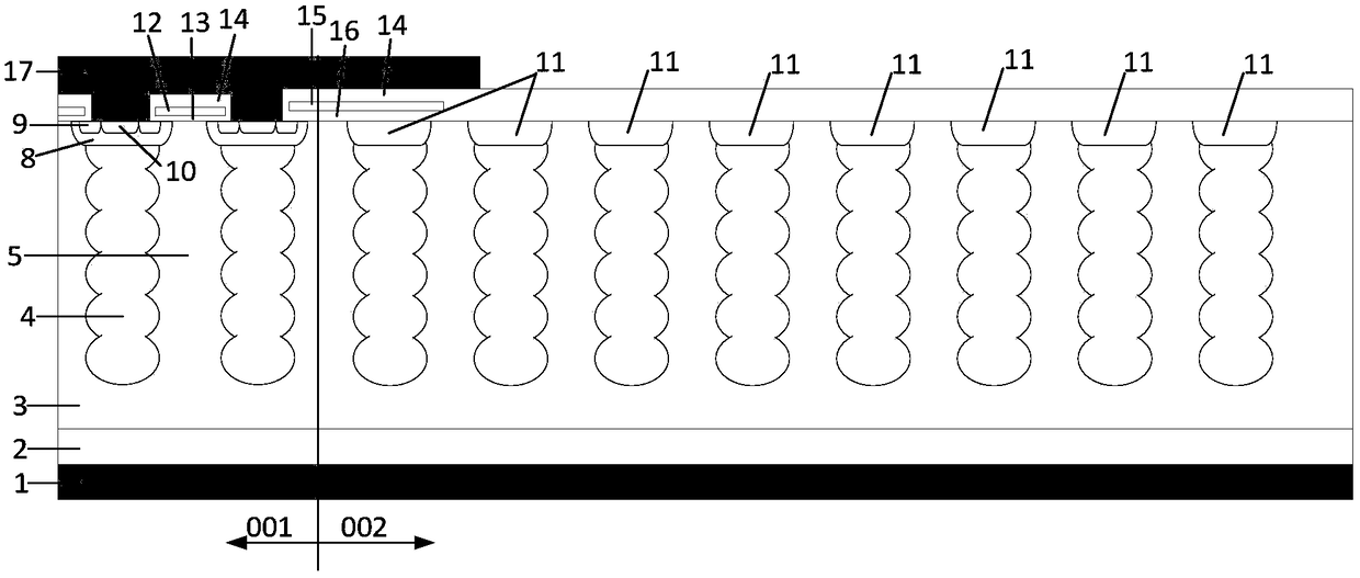
[0049] Embodiment 1: as figure 2 As shown, taking an N-type planar gate DMOS device as an example, the first conductivity type is N-type, and the second conductivity type is P-type. It is a multi-epitaxial super junction terminal structure. On the top view plane, the semiconductor The device includes an active area 001 and a terminal area 002 surrounding the active area 001;

[0050] In cross-sectional view, the terminal region 002 includes a drain metal 1, an N-type substrate 2 on the drain metal 1, and an N-type epitaxial layer 3 on the N-type substrate 2, and the N-type epitaxial layer 3 is provided with a number of P-type circular areas 6 regularly arranged in a ring shape, and adjacent P-type circular areas 6 are adjacent, and N-type areas 7 are provided between adjacent P-type circular areas 6; Three P-type well regions 11 are arranged on the surface of the terminal region 002 close to the active region 001;

[0051] A field oxide layer 16 is provided on the surface o...

Embodiment 2

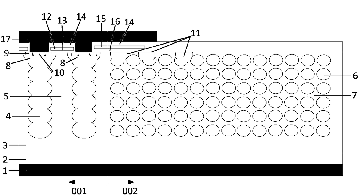
[0068] Embodiment 2: as image 3 As shown, taking an N-type planar gate DMOS device as an example, the first conductivity type is N-type, the second conductivity type is P-type, a super junction terminal structure with multiple epitaxy, and on the cross-sectional section, the The terminal region 002 includes a drain metal 1, an N-type substrate 2 on the drain metal 1, and an N-type epitaxial layer 3 on the N-type substrate 2. The N-type epitaxial layer 3 is provided with several regular rows An annular P-type circular area 6 is arranged, and the adjacent P-type circular areas 6 are spaced apart, and an N-type area 7 is provided between adjacent P-type circular areas 6; near the terminal area 002 there is Three P-type well regions 11 are provided on the surface of the source region 001;

[0069] In this embodiment, the boundaries of the upper and lower adjacent and left and right adjacent P-type circular regions 6 are phase-separated, and the P-type region of the active region...


PUM


Abstract

The invention belongs to the technical field of manufacturing semiconductor devices, and relates to a multi-epitaxial super-junction terminal structure. The multi-epitaxial super-junction terminal structure comprises a first conductive type epitaxial layer. In a terminal region, a plurality of regularly arranged circular second conductive type circular regions are arranged in the first conductivetype epitaxial layer, and adjacent second conductive type circular regions may be adjacent or separated, and a first conductive type region is disposed in an adjacent second conductive type circular interval; and a plurality of second conductive type well regions are disposed on the surface, of the terminal region, close to an active region. By setting the second conductive type circular (or elliptical) regions in the epitaxial layer of the terminal region, configuring the second conductive type circular regions to be adjacent or separated and setting a plurality of second conductive type circular regions for preventing breakdown on the surface close to the active region, the multi-epitaxial super-junction terminal structure enables the device to have higher withstand voltage efficiency inlateral withstand voltage and more complete depletion, thereby reducing the terminal area, reducing the overall chip area, reducing the production cost, and improving the cost performance of the chip.

Description

technical field [0001] The invention relates to a terminal structure of a semiconductor device and a manufacturing method thereof, in particular to a multi-epitaxial superjunction terminal structure and a manufacturing method thereof, belonging to the technical field of manufacturing semiconductor devices. Background technique [0002] The on-resistance of traditional power MOSFET devices is mainly determined by the length and doping concentration of the drift region. The smaller the length of the drift region, the smaller the on-resistance, and the higher the doping concentration of the drift region, the smaller the on-resistance. However, changes in these two aspects will lead to a decrease in the breakdown voltage of the device, so the on-resistance and the breakdown voltage are in a contradictory relationship or a compromise relationship, that is, the reduction of the on-resistance is limited by the breakdown voltage. [0003] The emergence of superjunction structures br...

Claims


Application Information

Patent Timeline
Patent Type & Authority Applications(China)
IPC IPC(8): H01L29/06
CPCH01L29/0634
Inventor 朱袁正周锦程李宗清
Owner WUXI NCE POWER
Why Eureka
Try Eureka