3D-RESURF terminal structure of power semiconductor device and manufacturing method thereof

A technology of power semiconductors and terminal structures, applied in semiconductor devices, electrical components, circuits, etc., can solve problems such as low chip area efficiency, large space area, and cost reduction, and achieve improved chip area efficiency, electric field concentration relief, and reduced requirements. Effect

Inactive Publication Date: 2017-11-03
UNIV OF ELECTRONICS SCI & TECH OF CHINA
View PDF4 Cites 5 Cited by
  • Summary
  • Abstract
  • Description
  • Claims
  • Application Information

AI Technical Summary

Problems solved by technology

To achieve high withstand voltage, this type of extended terminal requires a large space area, and the chip area efficiency is low, which is not conducive to reducing costs

Method used


Image

  • 3D-RESURF terminal structure of power semiconductor device and manufacturing method thereof
  • 3D-RESURF terminal structure of power semiconductor device and manufacturing method thereof
  • 3D-RESURF terminal structure of power semiconductor device and manufacturing method thereof

Examples


Embodiment 1

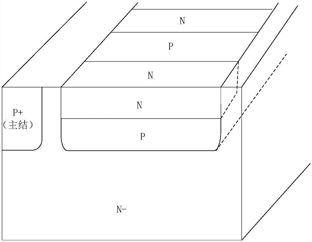
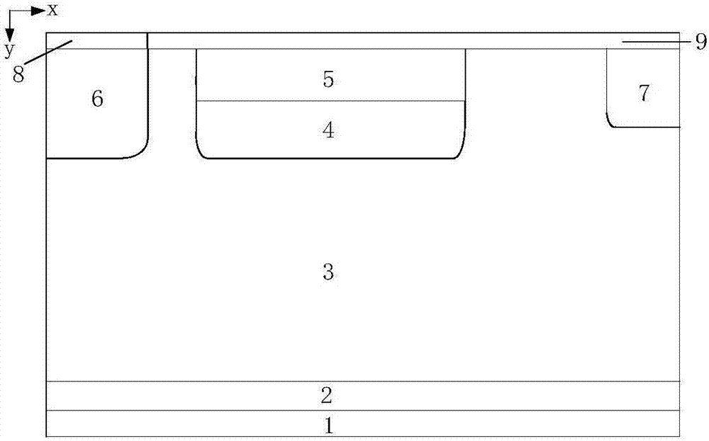
[0033] Such as figure 1 As shown, a 3D-RESURF terminal structure of a power semiconductor device includes a metalized cathode 1, a heavily doped semiconductor substrate of a first conductivity type above the metalized cathode 1, and a heavily doped first conductivity type from bottom to top. The first conductivity type lightly doped drift region 3 above the semiconductor substrate 2; the upper surface of the first conductivity type lightly doped drift region 3 is a field oxide layer 9; the interior of the first conductivity type lightly doped drift region 3 The upper left part is the second conductivity type semiconductor main junction 6; the upper surface of the second conductivity type semiconductor main junction 6 is connected to the metallization anode 8; the upper right part of the interior of the first conductivity type lightly doped drift region 3 is the first conductivity Type heavily doped stop ring 7; located between the second conductive type semiconductor main juncti...

Embodiment 2

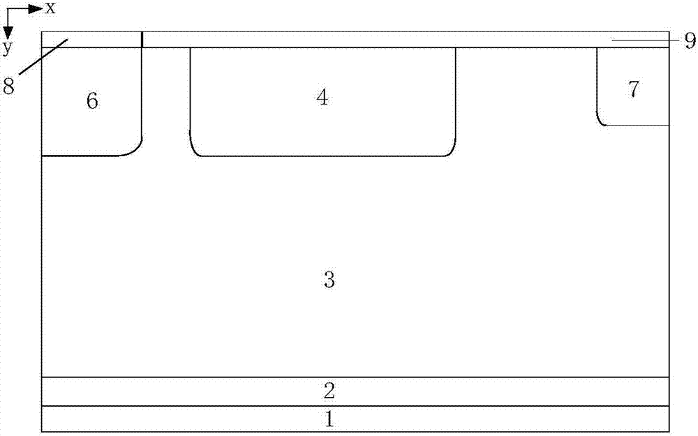
[0051] Such as Picture 12 As shown, this embodiment is basically the same as Embodiment 1, except that the first conductivity type semiconductor drift regions 5 are continuously arranged in the Z direction. When the first conductivity type semiconductor drift region 5 is continuous in the Z direction, the same photolithography is used when preparing the first conductivity type semiconductor drift region 5 and the second conductivity type semiconductor RESURF layer 4.

[0052] The semiconductor surface of this embodiment has no electric field component in the z direction, and its effect is slightly worse than that of Embodiment 1. However, this embodiment can be used when preparing the second conductivity type semiconductor RESURF region 4 and the first conductivity type semiconductor drift region 5 The same lithography plate, thereby reducing manufacturing costs. At the same time, this embodiment adopts the same preparation process as in embodiment 1. As the diffusion process is...

Embodiment 3

[0054] Such as Figure 13 As shown, this embodiment is basically the same as Embodiment 1, but the difference is that there are multiple first conductivity type semiconductor regions 5 above the second conductivity type semiconductor RESURF region 4, and the first conductivity type semiconductor drift region 5 is in the X direction and None are arranged continuously in the Z direction.

[0055] The structure proposed in this embodiment can better control the total amount of impurities, achieve charge balance, and completely deplete the surface; at the same time, the structure can change the surface to a certain extent by adjusting the distribution of the first conductivity type semiconductor region 5. The peak position of the electric field achieves higher withstand voltage.


PUM


Abstract

The invention provides a 3D-RESURF terminal structure of power semiconductor device and a manufacturing method thereof. The 3D-RESURF terminal structure comprises a metallizing cathode, a first conduction type heavily-doped semiconductor substrate, a first conduction type lightly-doped drift region, a field oxidation layer, a second conduction type semiconductor main knot and a first conduction type heavily-doped cut-off ring, wherein a second conduction type semiconductor RESURF layer is positioned between the second conduction type semiconductor main knot and the first conduction type semiconductor cut-off ring; a first conduction type semiconductor drift region is arranged above the second conduction type semiconductor RESURF layer. The second conduction type semiconductor lightly-doped RESURF layer near the second conduction type semiconductor main knot and the first conduction type semiconductor drift region above the second conduction type semiconductor main knot are exhausted mutually, a space charge region is formed, electric fields in y direction and z direction are introduced, and the distribution of the electric field in x direction is changed, so that triangular distribution of the electric field on the surface in x direction are changed into approximately trapezoidal distribution, the peak value of the electric value is reduced, and the breakdown voltage is improved.

Description

Technical field [0001] The invention belongs to the field of semiconductor technology, and relates to a terminal structure of a power semiconductor device and a manufacturing method thereof. Background technique [0002] The ability of power devices to block high voltage is mainly limited by the withstand voltage of the edge cell PN junction. The PN junction formed by diffusion will form a cylindrical junction at the edge of the diffusion window, and the diffusion at the four corners of the rectangular diffusion window will form a spherical junction, causing the breakdown voltage of the PN junction to be lower than the parallel plane junction voltage. At the same time, due to the influence of the interface charge, the surface electric field of the surface semiconductor is usually higher than the internal electric field, so that the avalanche breakdown of the chip occurs on the surface. The junction terminal is a special structure specially designed to reduce the local electric f...

Claims


Application Information

Patent Timeline
Patent Type & Authority Applications(China)
IPC IPC(8): H01L29/06
CPCH01L29/063H01L29/0623H01L29/0634
Inventor 任敏谢驰苏志恒林育赐李泽宏张波
Owner UNIV OF ELECTRONICS SCI & TECH OF CHINA
Why Eureka
Try Eureka